Software Modules Development
Welcome to the software development section of our Digital Signal Processing in MIMO and Dispersive Systems project. This part of our website serves to chronicle the journey of our software development, starting from the foundational work laid out in a master's thesis by one of our students, in collaboration with Infineon Austria, and extending into our current project, which aims to build upon and enhance this initial research.
Throughout this chapter, you will find detailed accounts of our software development process, from the initial stages rooted in academic research to the more complex and nuanced developments in our ongoing project. We aim to provide transparency in our progress, showcasing the challenges we've faced and the solutions we've crafted along the way.
As our project continues to evolve, we will update this section with the latest advancements in software development, reflecting both the growth of our team's expertise and the ongoing partnership with Infineon Austria.
Advancement: The Current Project with Infineon Austria
Building on the insights gained from the master's thesis of Mr.Gneist, our current collaboration with Infineon Austria seeks to further refine and expand these software capabilities. This section highlights the enhancements and new developments made to the existing software framework. We focus on the integration of more advanced algorithms, optimization of existing code, and the implementation of new features to meet the evolving needs of our research.
Enhanced LiteKit Software Architecture (by Mr. Anderle / Mr. Tenta 2024)
As the number of microphones increased to six, adapting the previous software architecture led to system crashes due to memory constraints. Reducing the buffer size per channel provided a functional but slow transmission. A new software approach was necessary to handle the increased data load efficiently.
Optimized Buffer Management for Real-Time Data Flow
To ensure a throughput fast enough to handle data from six microphones in quasi-real-time, the software logic and buffer management were completely reworked. The new buffer structure consists of two buffers: Buffer_A and Buffer_B. Each buffer contains 12,000 sint16 values, with 2,000 values allocated for each of the six channels. This dual-buffer approach mitigates delays, allowing one buffer to be filled with data while the other buffer is sent via UDP.
When the EDSADC indicates that a new value is ready, the interrupt service routine calls the corresponding function EDSADC_INTERRUPT_0(), as shown in the figure below.
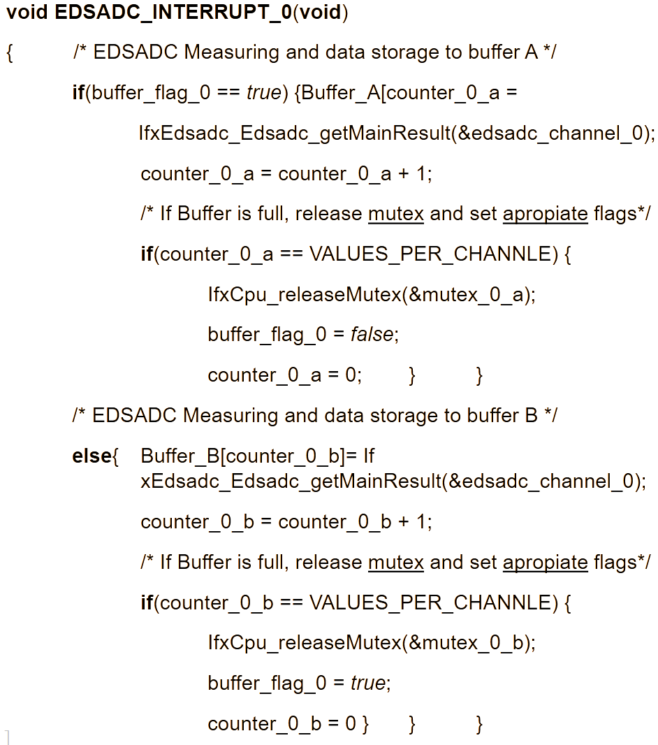
In the function, buffer_flag_0 is evaluated. If it's true, Buffer_A is used. The result from IfxEdsadc_Edsadc_getMainResult(&edsadc_channel_0) is written into Buffer_A at the location defined by counter_0_a, which ranges from 0 to 1,999. When counter_0_a reaches 2,000, Buffer_A is full, and IfxCpu_releaseMutex(&mutex_0_a) signals this to core0. Then buffer_flag_0 is set to false, and Buffer_B is used from this point forward. Finally, counter_0_a is reset to 0.
In subsequent calls of EDSADC_INTERRUPT_0(), buffer_flag_0 will be false, meaning Buffer_B is used. This functionality applies to all six interrupt service routines, with the only variation being the accessible range of each buffer.
Core0 Optimization for Efficient Data Transmission
The second significant change was reducing the code in Core0. Besides the initialization code for LwIP, the only remaining functionality handles the transmission of Buffer_A and Buffer_B. The figure below shows the code for transmitting Buffer_A over UDP.
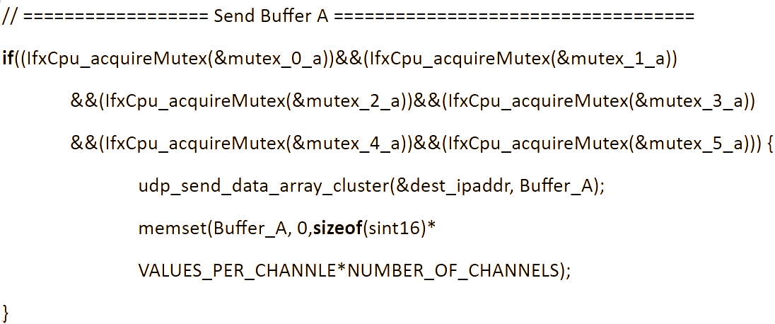
Once all six channels fill their allocated space in Buffer_A, all six mutexes are released. The if condition then becomes true, and Buffer_A is transmitted over UDP. Following this, all elements of Buffer_A are reset to 0 using memset(). The logic for Buffer_B is identical to that of Buffer_A.
Advanced Signal Processing and Data Handling in Matlab (by Mr. Anderle / Mr. Tenta 2024)
The Matlab script was adapted to accommodate the new buffer structure. Additionally, the script was refactored to group logically related code segments into dedicated functions, making the signal processing workflow more modular and efficient. A recording function was also integrated to streamline data capture for analysis.
Refined Data Naming and Modularization
The naming scheme for variables, functions, and comments was overhauled to accurately reflect the physical nature of the measured values. For example, PhaseShift was renamed to PhaseAngleDelta to better align with the technical context. Additionally, the script was made adaptable, supporting between one and six channels, which allows flexibility in configurations depending on the experimental setup.
IQ Demodulation and Filtering
As the data is separated by channel, IQ demodulation can be performed. Each of the following steps is applied to all 6 channels. To reduce the computational complexity, the sample rate is reduced from 156250 Hz to 15625. In addition, the atan2() function is used to handle the discontinuities that occur with the standard atan() function.
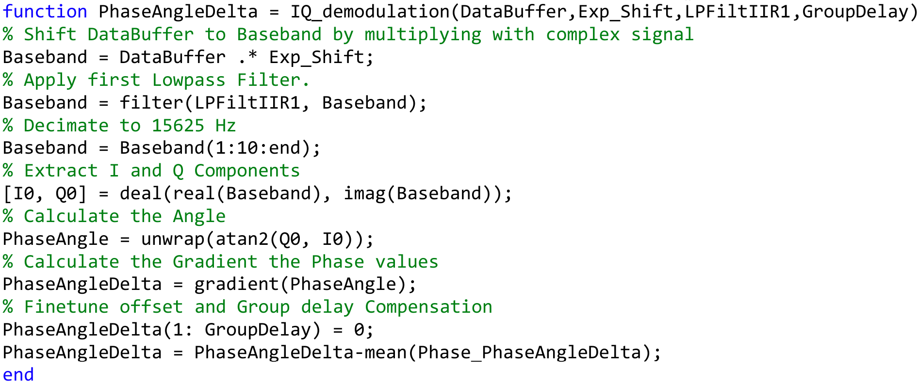
In the previous attempts, the resample() function was used. This function is computationally expensive. A comparison between resample(), decimate(), and using every 10th sample showed only small differences. Therefore, it was decided to use the less accurate but much cheaper option of simply copying every 10th sample.
The IIR filters used previously have much better performance than the higher-order FIR filters. The remaining values in the buffer are symmetrically centred around 0. The frequency of the low pass filters has been adjusted to achieve a good balance between noise suppression and preservation of the measured signals. The combination of the improved LPFiltIIR1 and reduced sampling frequency eliminates the need for LPFiltIIR2. After demodulation and filtering, the PhaseAngleDelta buffer contains the phase angle differences between the signal extracted from the I and Q signals.
Signal Processing in Matlab (by Mr. Anderle/ Mr. Tenta 2024)
Matlab is used to separate the data buffer received via UDP into individual channel buffers. Each of these channel buffers is filtered and IQ-demodulated. Additionally, a resampling stage is applied to reduce the sampling frequency, thereby decreasing the computational complexity.
UDP Data Separation
Each UDP datagram contains 4000 sint16 values per channel, totaling 12000 sint16 values per datagram. The concatenated channel data must be split into separate buffers, known as DataBuffers, for each channel. With a sampling rate of 156250 Hz, each DataBuffer holds 156250 sint16 values, representing 1 second of audio samples.

IQ Demodulation and Filtering
As the data is separated by channel, IQ demodulation can be performed. Each of the following steps is applied to all 3 channels. To reduce computational complexity, the sample rate is decreased from 156250Hz to 12500Hz using the resample() function. Additionally, the atan2() function is used to handle the discontinuities that occur with the standard atan() function.
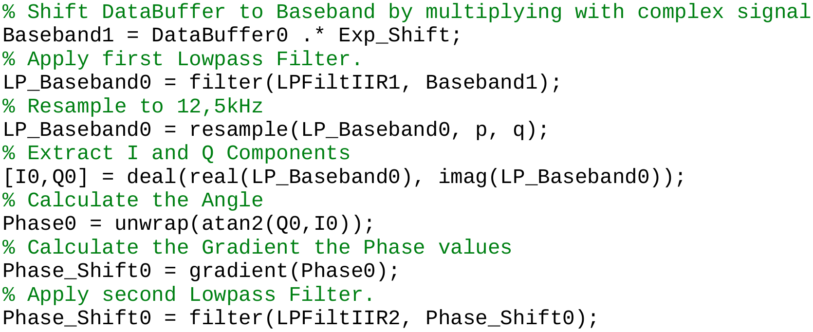
To manage computational complexity, we used second-order IIR filters instead of high-order FIR filters. However, due to the group delay introduced by IIR filters, the first 500 values are unusable and are set to 0. The remaining values in the buffer are symmetrically centered around 0.

After demodulation and filtering, the Phase_Shift0 buffers contains the phase shift changes between the I and Q signals. In the absence of movement at time t, there is no phase shift, resulting in Phase_Shift0[t] = 0. Movements away from the measuring head generate a negative phase shift, while movements toward the measuring head create a positive phase shift.
Further improvements to the Aurix LiteKit Software implementation - fine tuning the EDSADC configuration (Mr. Anderle 2024)
The current Aurix software allowed for a basic analysis of the signal chain. As detailed in previous section of this website, a frequency analysis of the transmitted values revealed an error of just under 4%. This error can be attributed to the method used for the Enhanced Delta-Sigma Analog-to-Digital Converter (EDSADC) measurements. Due to the absence of a direct interrupt callback structure in the EDSADC library, a timer was employed to trigger measurements at regular intervals. However, the EDSADC internally operates with oversampling and filtering. When the internal timings of the EDSADC do not aline with those of the external timer, a persistent error occurs. Therefore, it is essential to incorporate an interrupt callback structure.
Interrupt Callback
The Aurix TC375 does not have a readily usable interrupt service routine (ISR) for EDSADC. Therefore, the user must generate this structure. The steps below outline the procedure for implementing this ISR structure for EDSADC channel 0. The available service registers can be found in IfxSrc_regdef.h, but the documentation is lacking.
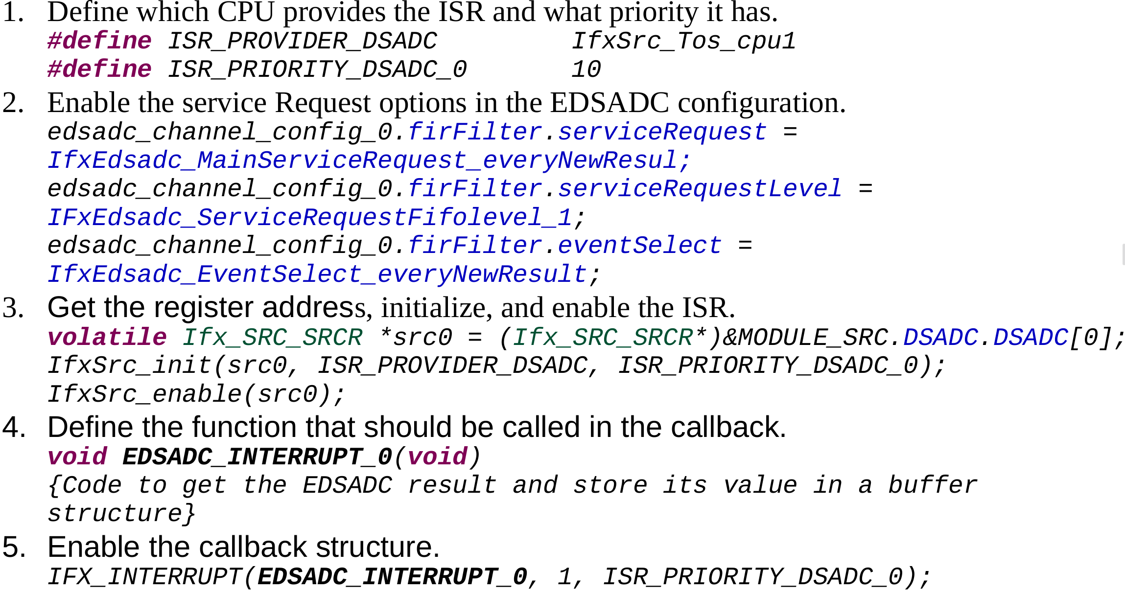
The same procedure is repeated for the other channels. The functions EDSADC_INTERRUPT_X() allow the EDSADC results to be read out with precise timing and no measurable error.
PWM Generation
To drive the ultrasound transducer on the UEB_V1, a PWM signal is produced. This is handled by Core2 of the LiteKit. The PWM generation code is derived from the gpt12_PWM example included in the Aurix Development Studio, with adjustments made to the parameters to fulfill the specific needs.

Enhanced Delta Sigma ADC (by Mr. Anderle/ Mr. Tenta 2024)
The Aurix TC375 LiteKit features 6 independent Delta Sigma ADCs (DSADC), called EDSADCs. During the evaluation process, only one channel is used.
EDSADC Overview
The sampling process of a signal with a DSADC involves three consecutive stages. In the first stage, the analogue input signal is sampled at a high frequency to generate a PDM signal. The second stage involves filtering the PDM signal with a lowpass filter. Finally, the signal's data rate is reduced with a decimator to simplify further processing. This overview shown the following figure is valid for all DSADCs.

Depending on the implementation of this general concept, additional modules are added at all points in the filter chain.
Aurix TC375 EDSADC
All 6 channels of the DSADC Module implement the same filter chain, as shown in the following figure.
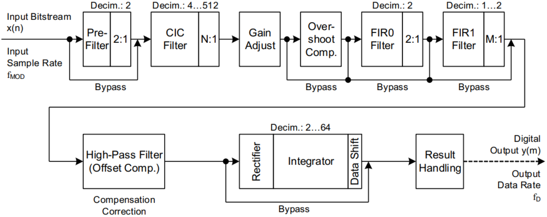
The input Bitstream x(n) is the sampled PDM signal from the modulator. Channel 1 of the EDSADC Module is used and the filter chain is configured with the settings shown in the following Table.

With these base parameters and the application specific parameters FM and AFS, two additional settings can be calculated which are necessary for the proper initialization of the module.
The CICSHIFT and the GAINFACTOR.
FM: Modulator gain factor (when using the on-chip modulator FM = 0.6945)
AFS: Intended calibrated full-scale value. At 3.3V this is 30000.
N: Decimation Ratio or decimation Factor.
CICSHIFT = roundup(14 − log2(2 * AFS / (N^3 * 4 * FM))
GAINFACTOR = truncate(((2 * AFS / N^3 * 4 * FM ) * 2^(CICSHIFT - 14))*4096)
With the use on-chip modulator FM =0.6945, at 3.3V the AFS is 30000 and the decimation ratio is set to 32. This results in CICSHIFT of 15 and a GAINFACTOR of 5399.
EDSADC Initialization Values
As all required variables are known the module is initialized as edsadc_module_handler with the channel 1 handler edsadc_channel_1. The differential input pins are AN37 and AN38.
edsadc_channel_config_1.modulator.modulatorClockFreq = 40e6;
edsadc_channel_config_1.combFilter.decimationFactor = 32;
edsadc_channel_config_1.firFilter.prefilterEnabled = FALSE;
edsadc_channel_config_1.firFilter.fir0Enabled = FALSE;
edsadc_channel_config_1.firFilter.fir1Enabled = FALSE;
edsadc_channel_config_1.channelId = 1;
edsadc_channel_config_1.cicShift = 15;
edsadc_channel_config_1.gainFactor = 5399;
edsadc_channel_config_1.gainCalibrationConfig.calTarget = 30000;
edsadc_channel_config_1.modulator.positiveInput = IfxEdsadc_InputConfig_inputPin;
edsadc_channel_config_1.modulator.negativeInput = IfxEdsadc_InputConfig_inputPin;
To start the EDSADC the Modulator Mask and Channel Mask are each set to 0x2 or 0b00000010, with IfxEdsadc_Edsadc_startScan(&edsadc_module_handler,0x2, 02);
EDSADC Validation
The ILLD TC37A Version: 1.0.1.16.0 only provide a basic implementation of the EDSADC. There is a IfxEdsadc_Edsadc_getMainResult() function present, but there are no debugging functions in the recommended IfxEdsadc_Edsadc.h , which complicated the validation process. In the underlying IfxEdsadc.h where undocumented functions, as shown in the following table.

With these functions it was possible to check the initial settings validity and to determine the group delay of the EDSADC with the chosen parameters. The validation process shows that the main_comb_out_frequency is 1.25MHz. This is expected as the Modulator frequency is set to 40MHz and the Decimation Ratio is 32; 40MHz/32 = 1.25MHz.
The other results were in line with expectations, whereby the main_group_delay with a value of 1.2uS will be particularly interesting for a later “maximum capability” analysis of the EDSADC. Since we only intend to measure signals up to 50kHz, a sampling rate of 1.25MHz is excessive in the long term, but it is well suited for validation, since a 50kHz sine wave can be optically recognized with such a high oversampling as shown in the figure below.
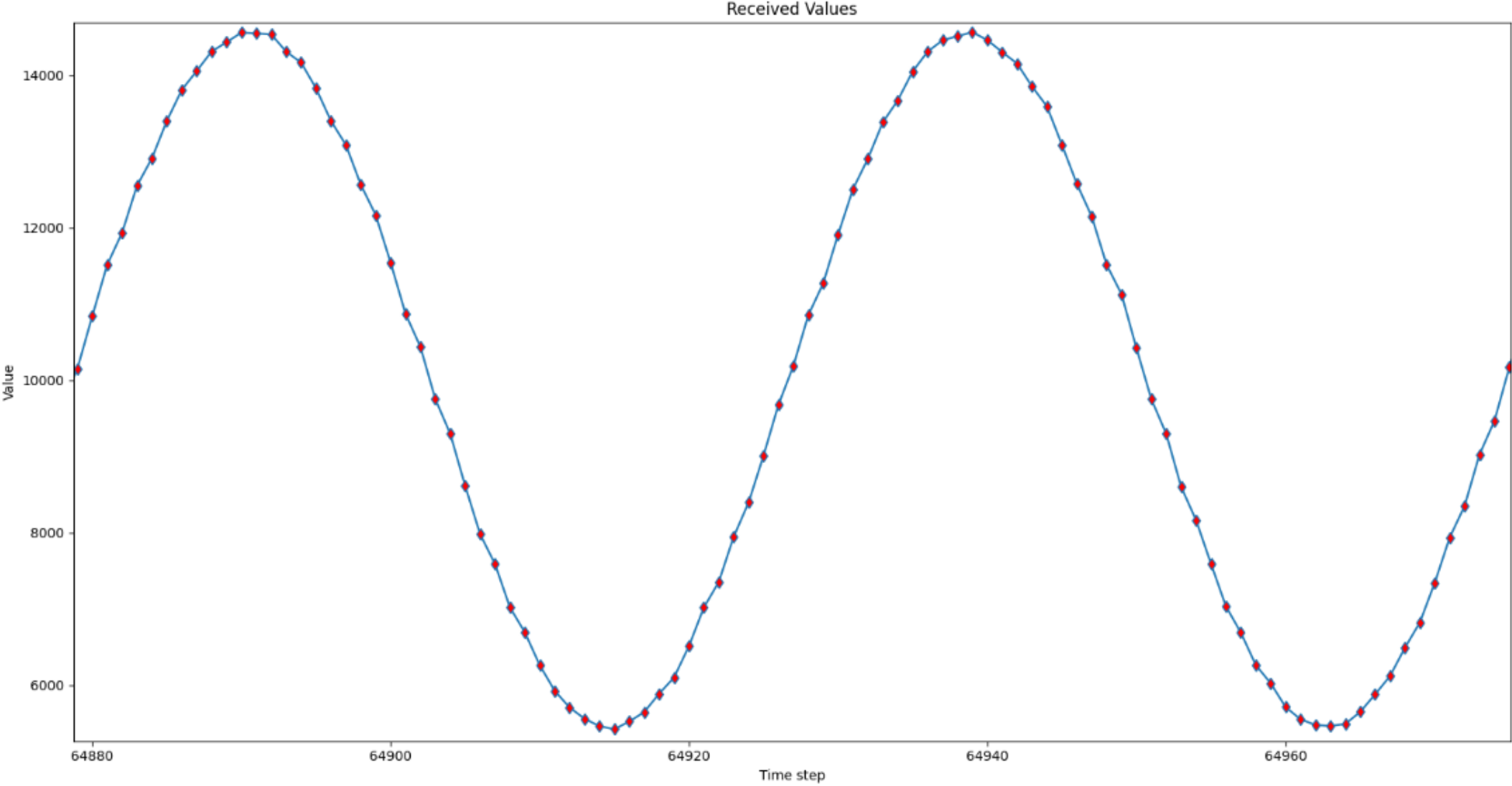
The sine wave shown was generated with a frequency of 50kHz and an amplitude of 1Vpp. To protect the EDSADC from negative voltages, an additional DC component of 1.095V was applied. This DC component corresponds to 10000 on the rating scale, this means that 10000 is the zero line.
EDSADC Result Evaluation
The EDSADC result is obtained with the call of the function IfxEdsadc_Edsadc_getMainResult(). As the EDSADC does not provide a easy to use interrupt function or callback handler to obtain the result, it is necessary to implement the handling and timing for the result acquirement function.
Basic Wait Loop
The first approach to obtain the EDSADC result in a defined way was an iterative approach. With several wait(n) functions provided by the ILLD, the timing is manipulated so that the results match the input signal. A 50kHz sine wave was fed into the EDSADC, and the results were analysed. If the signal pattern and the FFT were wrong, the wait parameter was changed, and the evaluation started again. This approach has two major drawbacks: First, the timing changes with every change in the code. Second, with different sample frequencies, the timing constants changed slightly. The difference from the measured value to the true frequency of the input signal was 3.8% for 100Hz and 4.3% for 50kHz. However, the frequency of the measured values was always lower than the original signal frequency.
Timer Triggered Interrupt
To mitigate the drawbacks of the “Basic Wait Loop”, the GPT12 Timer was used. The timer is initialized with the RELOAD_VALUE and two separate prescalers. The three values, shown further below, determine the interrupt frequency F of the GPT12 with the following calculation:
RELOAD_VALUE = 100MHz/(PRE1 *PRE2*F).
To visually recognise a sine wave, 10 datapoints are enough, so the GPT12 interrupt has a frequency of 500kHz. This leads to a REALOAD_VALUE of 50.
PRE1 --> IfxGpt12_Gpt1BlockPrescaler_4
PRE2 --> IfxGpt12_TimerInputPrescaler_1
F --> 500kHz
With this timer parameter, the GPT12 is initialized with its otherwise default configuration.
Timer Triggered Results
For the evaluation of this approach 5 sine waves with different frequencies were generated. The Vpp of 1V and the DC Offset of 1.095 remained the same. As a pure optical recognition is not enough a MATLAB script is used to calculate the FFT of the measured samples.

As can be seen in the table above, the measured frequencies are too high, with approximately 3.85%, linear over the desired frequency range. It is unclear whether this error stems from the configuration of the EDSADC, interrupt timing or the MATLAB script.
Lightweight IP stack (lwIP) implementation on the Aurix platform (Mr. Tenta 2024)
The Lightweight IP stack (lwIP) is an open-source TCP/IP stack designed for embedded systems with limited resources. Adam Dunkels initially developed it at the Swedish Institute of Computer Science, and it has since become a popular choice for enabling network communication in a wide range of devices, from microcontrollers to small embedded systems. The primary goal of lwIP is to reduce memory usage andcode size, making it well-suited for systems where such resources are at a premium yet still providing a full-featured TCP/IP solution.
lwIP can be used in various embedded systems to add networking capabilities. It supports the major Internet protocols, including TCP, UDP, ICMP, and IP, along with several application-level protocols, such as DHCP and DNS. The stack is designed to be highly configurable, allowing developers to tailor it to their project's specific needs and constraints. Common use cases include:
Embedded Web Servers: Devices can host simple web interfaces for configuration or monitoring.
Internet of Things (IoT) Devices: Enables network connectivity for sensors, actuators, and other devices.
Networked Embedded Applications: For applications requiring remote control, data collection, or updates over the network.
lwIP provides several APIs for different use cases, ranging from lower-level to higher-level interfaces. These APIs allow developers to choose the most appropriate level of abstraction for their projects based on factors like the desired control level, memory usage, and ease of use. The main APIs are:
Raw API: The lowest-level API provides direct access to the core lwIP stack. It is non-thread-safe and requires the programmer's careful management of timing and state. This API is suitable for systems where maximum performance and minimum footprint are critical, and the developer is willing to manage more complexity.
Netconn API: This API is a higher-level API that abstracts some of the complexities of the raw API. It is designed to be easier to use while still being reasonably lightweight. The Netconn API is thread-safe and suitable for use in multi-threaded environments. It provides a sequential programming model and is often used for more straightforward applications where ease of use is a priority over the absolute lowest resource consumption.
Socket API: The highest level API, modelled after the BSD socket API, making it familiar to developers with experience in traditional network programming. This API is the easiest for those familiar with socket programming but incurs additional overhead compared to the lower-level APIs. The Socket API is thread-safe and suitable for porting existing network applications to lwIP with minimal changes.
RAW API
As the Netconn API and the Socket API need some operating system, only the RAW API is usable for the project. Here are the usage considerations:
Complexity: The trade-off for the efficiency and control offered by the RAW API is increased complexity in application code. Developers must understand the TCP/IP stack well and be prepared to manage more aspects of the networking operations manually.
Manual management: Unlike the Socket or Netconn APIs, which manage aspects like buffer handling, connection states, and retransmissions more automatically, the RAW API requires the developer to handle these tasks explicitly,which can lead to more complex application code but allows for optimizations specific to the application's requirements.
Event-driven programming: The RAW API operates on an event-driven model, where callbacks notify the application of network events (e.g., incoming data, state changes). This model requires a different program structure approach than the blocking I/O model used in traditional socket programming.
Typical Use Cases are:
Custom protocol implementation: Application-specific protocol is needed when standard protocols are unsuitable or highly optimized.
Maximum performance: In scenarios where achieving the lowest possible latency and highest throughput is critical.
Extremely resource-constrained devices: If the overhead of higher-level APIs cannot be tolerated due to limited memory or CPU resources.
In summary, the RAW API of lwIP offers the highest level of efficiency and control for embedded network applications but requires careful management and a solid understanding of the TCP/IP stack due to its complexity and non-thread-safe nature. It is an excellent choice for specialized applications where the overhead of more abstracted APIs is unacceptable.
Implementation on the Aurix TC375
On the Aurix TC375, the lwIP is implemented and executed on core 0. Core 1 is responsible for Delta-Sigma measurements. The following figure shows the layout of the Aurix TC375 program.
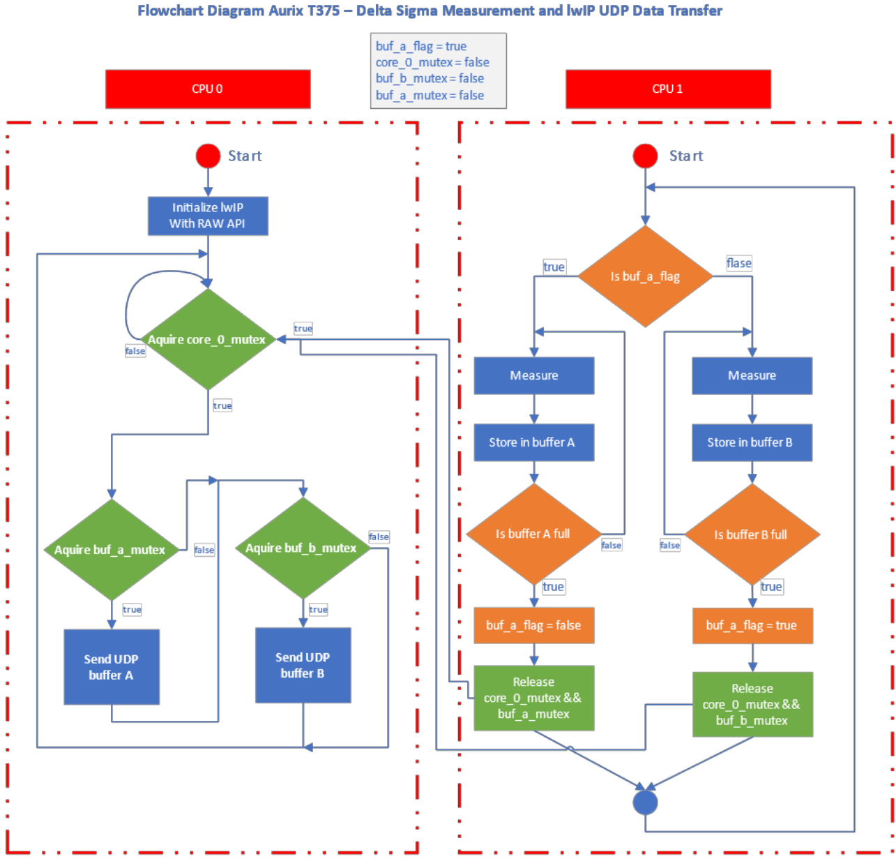
1. After lwIP is initialized on CPU 0, the core will block in a while loop,
trying to acquire the core_0_mutex, which is set to zero initially.
2. CPU 1 will start filling buffer A with measurement data because the
buffer_a_flag is true when the program starts.
3. When the buffer is full, CPU 1 will signal to CPU 0 that the buffer is
ready to be sent via UDP by releasing core_0_mutex and
buf_a_mutex. CPU 0 sends the buffer and blocks again in the while
loop, waiting to acquire core_0_mutex.
4. CPU 1 will switch to buffer B by setting the buf_a_flag to false. When
buffer B is full, CPU 1 signals CPU 0 to send the buffer by releasing
core_0_mutex and buf_b_mutex. Steps 2 to 4 are repeated
indefinitely.
To ensure that lwIP runs correctly, one should set the max lifetime of an entry in the address resolution protocol (ARP) to a high value. This can be done in the opt.h file (path: /Libraries/Ethernet/lwip/src/include/lwip/opt.h). The ARP_MAXAGE, which is 300 (5 minutes) by default, should be set to 4,294,967,295, the max unsigned integer value, thus ensuring that the communication between the Aurix board and the server stays long enough valid.
Interfacing the EDSADC modules of the Aurix LiteKit (by Mr. Anderle 2023)
As a first step into digitizing the analog signal from the MEMS microphone, the hardware was connected to the EDSADC module of the Aurix TC375.
The sampled data is than processed and sent via a USB-UART interface for further analysis.On the PC, this data is received by a MatLab program, processed and displayed as a
function of time.
The software on the Aurix LiteKit uses the Infineon Low-Level Driver to achieve the required functionality. This functionality can be divided into three successive parts. Initialization, measurement with conversion and transmission. During the initialization sequence, the function of the IfxAsclin_Asc library, namely the initUART(), is used to initialize a UART module. This module handles the data transfer from the microcontroller to the PC. As the next step, the library IfxEdsadc_Edsadc is used to initialize the EDSADC module. With init_EDSADC(), the module is configured so that the signals from the audio front end can be sampled fast and clean. This step completes the initialization, and the main() loop starts.
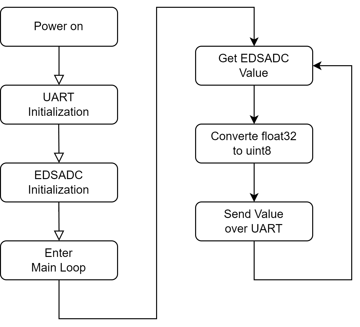
The flow chart above shows a visual description of the sequence. In each loop, the signal from the audio front end is sampled with the EDSADC via the IfxEdsadc_Edsadc_getMainResult() function. The result is then converted directly into a voltage value, a float32. Since the UART function, IfxAsclin_Asc_write() works with uint8 values, the float32 is scaled down for the fastest possible transmission. In addition, an offset is added to produce a voltage value with a lower resolution, which can be between 0V and 2.55V. This value is then sent to the PC with the UART Wrapper Function uart_sendMessage(). This value is then sent to the PC with the UART Wrapper Function uart_sendMessage().
MATLAB ADC Result Visualization (using a UART communication interface) (by Mr. Anderle/ Mr. Tenta 2023)
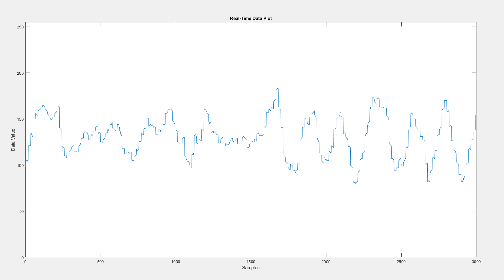
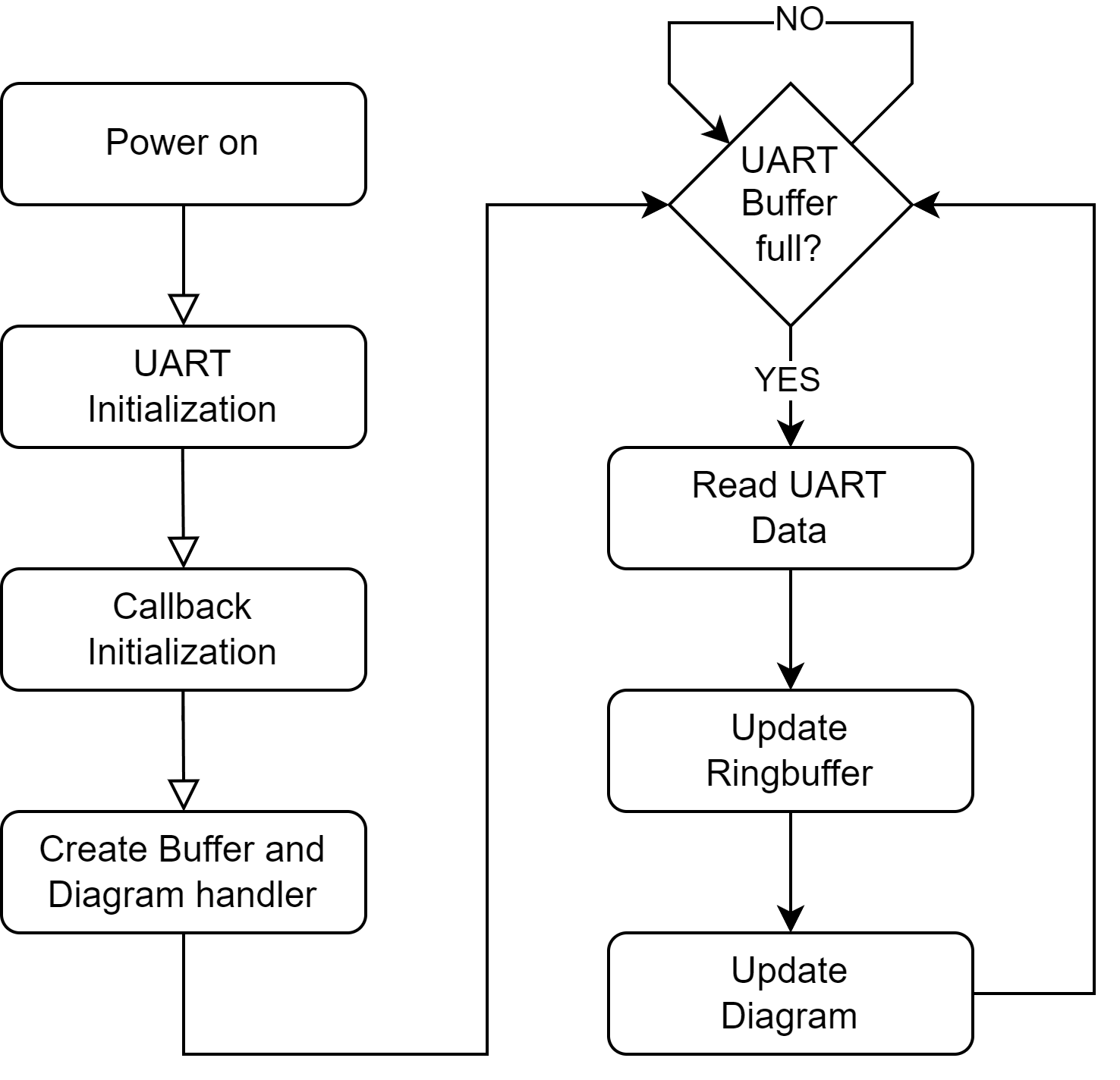
The MatLab program's objective is to obtain the values from the Aurix LiteKit and display them graphically. The first step is to set up a UART object and configure it with the matching COM port and baud rate. Then, a callback to the readUARTData function is set up. This allows the UART to be read in 32 byte bursts and thus reduces the load on the system compared to one byte at a time. A memory structure dataBuffer is created, which will be used as a ring buffer later. The last step of the setup is to establish the handler for the data visualization diagram hPlot. When 32bytes of data have been received via the UART interface, the callback to the readUARTData function is triggered. All available data is read from the UART and written to the end of the dataBuffer. Finally, the diagram is updated via the hPlot handler. This results in a signal moving from right to left, with the most recent values displayed on the right and the oldest values on the left, as shown in the following figure.
A visual description of the program sequence is shown in figure below.
Foundation: Infineon Aurix EVADCs data capture and processing transfer via TCP/IP and process via Matlab
(by Mr. Gneist 2022/23)
Key to the foundation of our project is the precise handling of audio signals through specialized hardware. The MEMS microphone used in our setup is characterized by a resonance at 35kHz, while the accompanying ceramic ultrasonic sending capsule, serving as our transmitter, operates at a center frequency of around 40kHz. This operating point around 40kHz is crucial for the synchronization of the transmitter and receiver components in our system.
The configuration comprises three MEMS microphones and one ultrasonic sender. These microphones are tasked with receiving sine wave signals of varying amplitudes, which are integral to our method of heart rate determination. An essential aspect of this process is a measurement duration of 60 seconds, which is based on the premise that such a duration is necessary for accurate heart rate analysis.
Adhering to the Nyquist-Shannon sampling theorem, we determined that a minimum sampling frequency of 80kHz is essential for reconstructing the frequency information of the original signal. To capture the shape of the original signal with higher fidelity, we operate at a sampling frequency ranging between 200kHz and 400kHz. Utilizing the capabilities of the Aurix platform, particularly its Enhanced Versatile ADC (EVADC), we achieve a conversion rate of 1.29MHz. This high conversion rate allows us to represent each sample with a 12-bit resolution, stored as unsigned 16-bit integer data types.
For evaluation and testing of various signal processing algorithms, we have developed a system to transfer the measurement data to a PC interface. This approach enables us to handle the large volume of raw data generated by the high conversion rates and prolonged measurement times without any compression. The following equation, presented later in this section, calculates the maximum data rate required for this interface, as well as the total amount of data for a 60-second measurement set. Such a system design ensures that the bandwidth of the setup is not a limiting factor, allowing for comprehensive data analysis and algorithm testing.

Reasons behind switching to the Aurix LiteKit Evaluation Board from the Shieldbuddy Board
First, the ShieldBuddy (SB) evaluation board has been considered for the realisation of this project. The first microphone front-end PCBs have been developed to be compatible with the SB. Besides, the evaluation of the maximum conversion rate, Synchronisation Groups and Alias Feature has been conducted first with the SB. For this evaluation and tests, a UART interface of the Aurix has been used in conjunction with a Python PC application. Later, due to the examinations taken as shown in the previous equation, the amount of data for one measurement set can no longer be stored on the Aurix all at once. Besides, the UART interface creates a bottleneck because its maximum data rate does not come along with the actual data throughput required by the high conversion rate and continuous transmissions. The following table compares the UART- and the Ethernet interface of the Aurix. It lists their maximum data rates in conjunction with the project requirements. The UART interface, even with operation outside of the specification, represents a limiting element regarding data throughput in this application. This explains the switch to the Aurix’ Ethernet interface and the switch to the LiteKit evaluation board as the ShieldBuddy does not provide an access to the Ethernet module.

Switching to the LiteKit for using the Ethernet interface brings several advantages. As Matlab provides an API for Ethernet TCP/IP communication, the data can be easily received from the LiteKit via a Matlab script on the PC. Matlab is platform independent, on every platform available and requires no additional drivers to enable the communication over Ethernet TCP/IP. The raw EVADC measure values are received and stored in Matlab what enables a lot of possibilities to apply as well as test several signal processing steps and algorithms to determine the heart rate in a non-invasive and contactless manner. From the Matlab Code it is feasible to generate C-Code for embedded hardware platforms what could be considered for the Aurix software to enable a final self-sufficient system. In this context, selfsufficient means that a PC connection is no longer necessary to measure the heart rate.
LiteKit and ShieldBuddy EVADC Resources
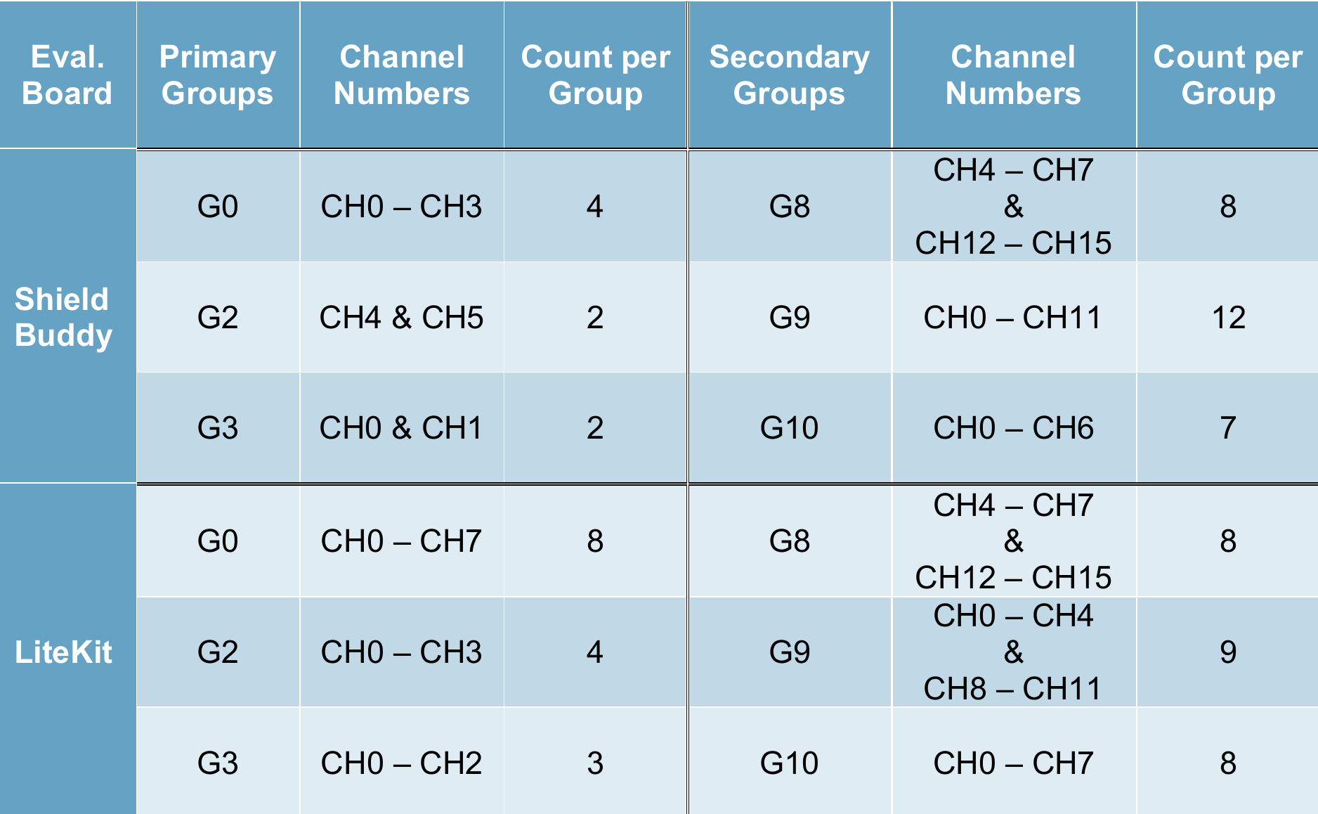
This section provides an overview of the Enhanced Versatile ADC (EVADC) resources available on both the ShieldBuddy and LiteKit evaluation boards. We have compiled a detailed table (shown below) that outlines the specific EVADC channels and their corresponding signals across these platforms. To determine the exact source and signal path for each EVADC channel, we have utilized information from the official datasheets. These datasheets detail the connectors and jumper positions for the input channels on both evaluation boards. It's important to note that some channels may overlap or share the same pin, affecting their simultaneous usability. For example, on the ShieldBuddy, certain channels cannot be used concurrently due to shared pins, and on the LiteKit, certain channels like G0 CH0 are available only under specific conditions, such as disassembling the onboard potentiometer. Furthermore, our analysis reveals that both the ShieldBuddy and LiteKit offer three primary and three secondary groups with at least two channels each for ADC conversions. These groups can be configured into a Synchronization Group to enable parallel conversions across multiple channels. While the ShieldBuddy may require the use of the Alias Feature for setting up these groups, the LiteKit's configuration allows for more straightforward group formations without necessarily relying on this feature. The nuances of forming Synchronization Groups and the application of the Alias Feature are explained in detail in our dedicated technical sections. The following table effectively illustrates the available resources and configurations for EVADC on these evaluation boards, providing a clear understanding of their capabilities in our project's context.
Microcontroller Firmware
The project takes full advantage of the tri-core architecture of the Aurix microcontroller by distributing software functions across all three cores. This multicore setup enhances efficiency and performance, as outlined in the illustration provided in the following figure.
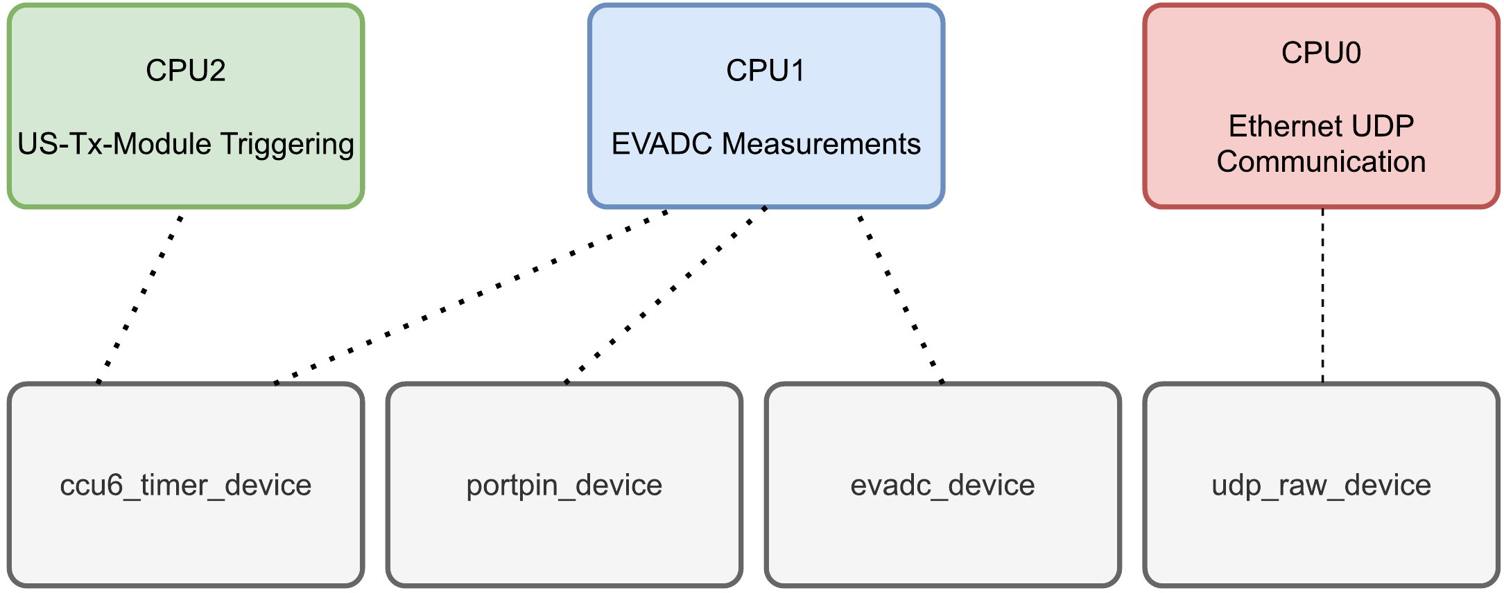
Each core within the Aurix microcontroller is assigned specific responsibilities. CPU1, in this application considered as the main core, is tasked with managing EVADC measurements and organizing the storage of sample values. It plays a pivotal role in controlling the software flow of the project. CPU0 is dedicated to handling Ethernet UDP communications, including the transmission of measurement packages as directed by CPU1. Notably, CPU0 and CPU1 share three memory resources, facilitating efficient data management and communication between them. Meanwhile, CPU2 operates independently, primarily responsible for generating PWM signals to trigger the ultrasound transmitter module (US-Tx-Module). While this section provides an overview of the core functionalities and interactions within our multicore setup, detailed information regarding the EVADC resources, configuration, and conversion timing, as well as specific measurement results, can be found in the technical documentation of our project.