Analog Front-End Design to Interface MEMS-based Microphones
Welcome to the hardware development section of our Digital Signal Processing in MIMO and Dispersive Systems project. This chapter outlines the evolution of our hardware, beginning with a master's thesis conducted in collaboration with Infineon Austria and progressing through to our ongoing project, which aims to further refine and extend this foundational work. It is essential to design and implement a robust analog circuit to ensure a consistent signal path from sonic waves hitting the MEMS microphones to sampling the signal at the Analog-to-Digital converters (ADCs). The MEMS microphones produce a differential signal which the analog front end has to amplify and shift into the range of the utilized Aurix ADCs. Designing the first prototype hardware and testing its capabilities led to further itterations of the front-end design. The version currently in use is V3. The basic principle for all revisions is the same. First get the differential signal from the microphone and amplify the signal using a operational amplifier. Importen here is that the signal path from the microphone to the opamp does not produce to much load on the microphone, preserves the signal integrity and also considers impedance and capacitence compensation. The opamp has to be choosen carefully to ensure an optimal signal for digitalization. As the output voltage swing from a MEMS microphone can vary greatly from a few mv peak-peak up to the applied supply voltage, it is required to carefuly choose and design the amplifier part of the circuit. Finally, the path from the amplified signal to the input of the ADC has to ensure a safe voltage range to not damage the input stage of the ADC.Improved Receiver PCB Design: AFE_V2 for Six Microphones (by Mr. Anderle 2024)
Our ongoing developments have demonstrated that a three-channel setup increases the accuracy of measurement results. With the Aurix TC375 microcontroller on the LiteKitV2 featuring more Delta-Sigma ADCs than previously used, the number of microphones is increased to six, fully utilizing the microcontroller's capabilities. The main objective of the AFE_V2 is to integrate all components of the receiver side onto a single PCB.
Updated AFE_V2 Schematic for Enhanced Signal Handling
The signal paths of the six microphones are shown in the figure below. The component selection and amplification stage for each microphone signal path follows a similar approach as used in the earlier AFE_V1 version.
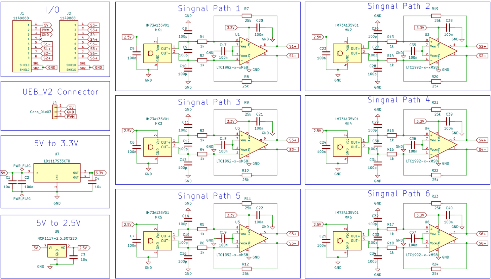
To enhance resilience against EMI, the connectors between AFE_V2 and LiteKitV2 (J1 and J2) were changed to shielded RJ45 sockets. As the AFE_V2 and the UEB_V2 are mounted on the same 3D-printed frame, the sensor head, the signal path of the PWM signal is routed over the AFE_V2 to shorten the length of unshielded wires.
Optimized AFE_V2 Layout for EMI Reduction and Beamforming
The layout design prioritizes EMI reduction and microphone positioning for beamforming. Signal paths are spaced adequately to dampen EMI, as shown in the figure below. For effective beamforming, the microphones are positioned in a linear array, with the spacing between two microphones less than half the wavelength of the signal frequency. Given the used frequency is 33333 Hz and the speed of sound in air is 343 m/s, the resulting mounting distance is approximately 5 mm. The spacing is measured from the middle of each microphone membrane (highlighted in light blue).
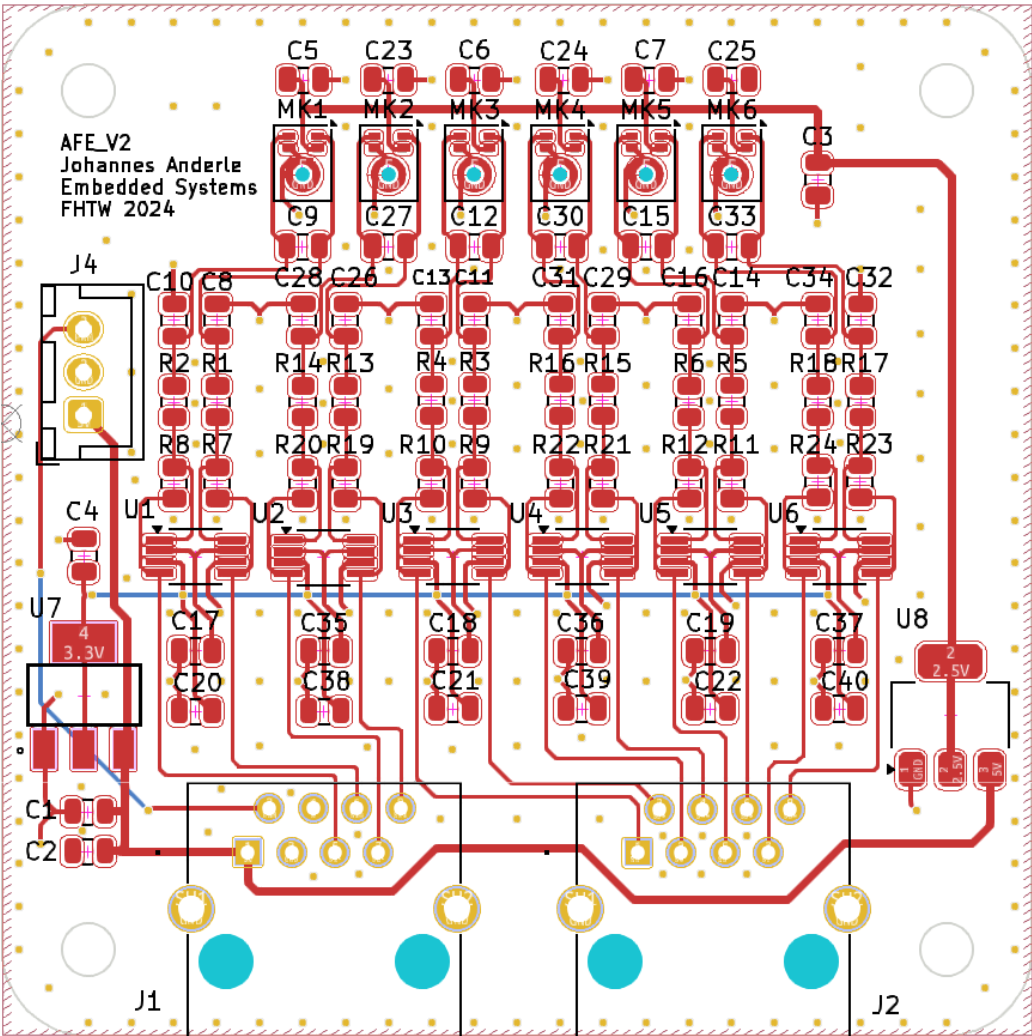
The physical arrangement of the microphones results in slight differences in signal path lengths. For example, the MK1 trace is 5 mm longer than KM5. Typically, such differences would require compensation by matching trace lengths. However, as the speed of an electrical signal is much faster than the speed of sound, this difference is negligible. The UEB_V2 is mounted on the left side of the sensor head, so connector J4 is placed on the left to minimize unshielded cable length. The figure below shows the assembled AFE_V2.
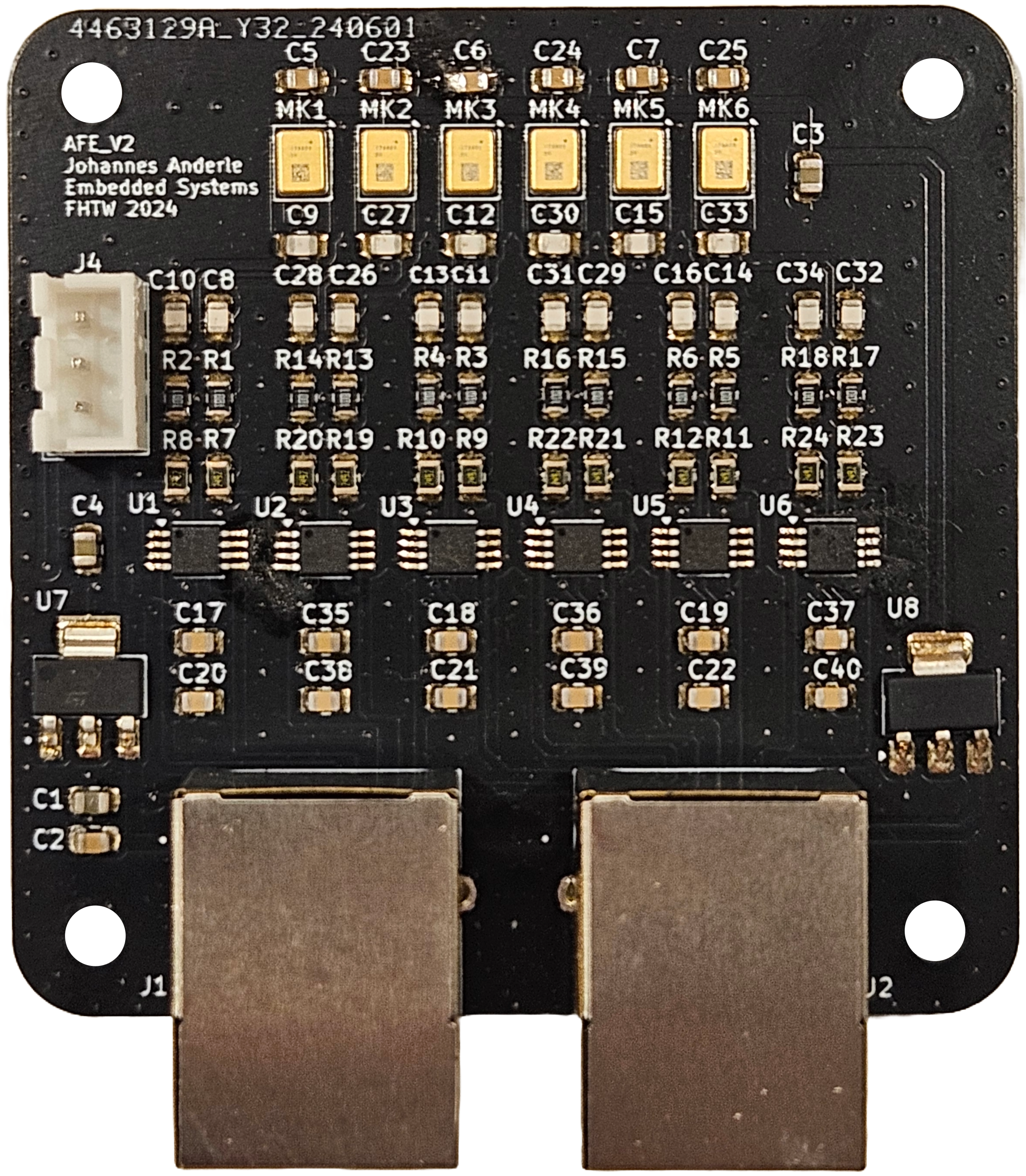
While the RJ45 sockets (J1 and J2) take up significant space on the PCB, they enable the use of standard Ethernet cables for EMI-resistant power and signal transmission, which justifies their inclusion despite the space they occupy.
Transmitter PCB: UEB_V2 Update and Miniaturization (by Mr. Anderle 2024)
Following the updates made to AFE_V2, the UEB_V2 is an improved version of UEB_V1.
UEB_V2 Schematic: Optimized for 3.3V Operation
Like the AFE_V2, the UEB_V2 is powered by 5V, although the entire circuit operates on 3.3V, which is provided by the LDO U2, as depicted in the figure below. This configuration reduces the risk of damaging the LiteKitV2 due to incorrect wiring.
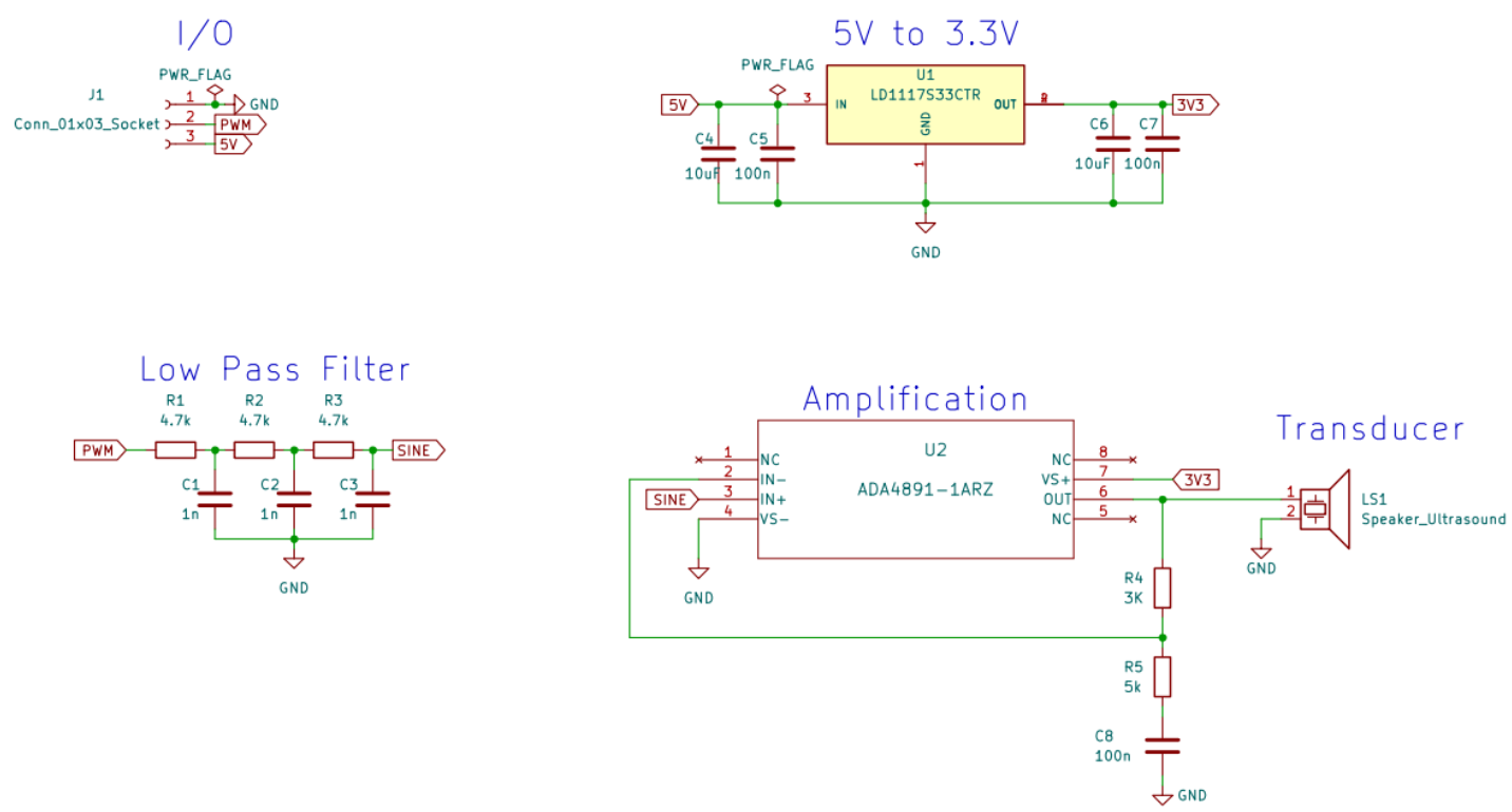
The LiteKitV2 output signal is a PWM signal, which is converted into an approximate sine wave through three low-pass filters connected in series (R1/C1, R2/C2, and R3/C3). The OPV U2, together with the external circuit R4/R5, provides the necessary energy for the ultrasonic transducer. All non-essential jumpers, measurement points, and components have been removed for simplification.
UEB_V2 Compact Layout and Component Simplification
The layout emphasizes size reduction and component assembly simplicity. Compared to the UEB_V1, the layout has been greatly simplified, as shown in the figure below.
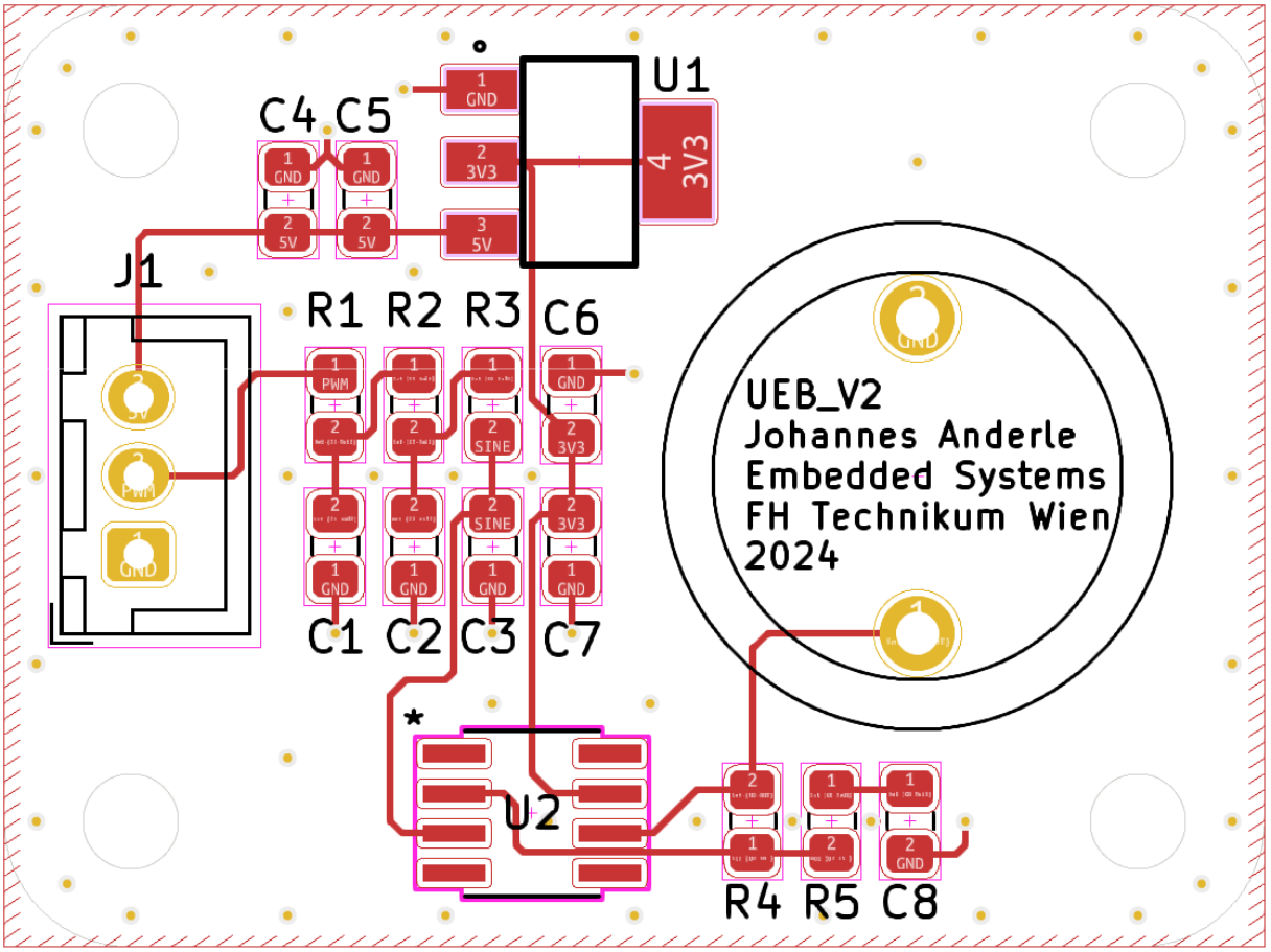
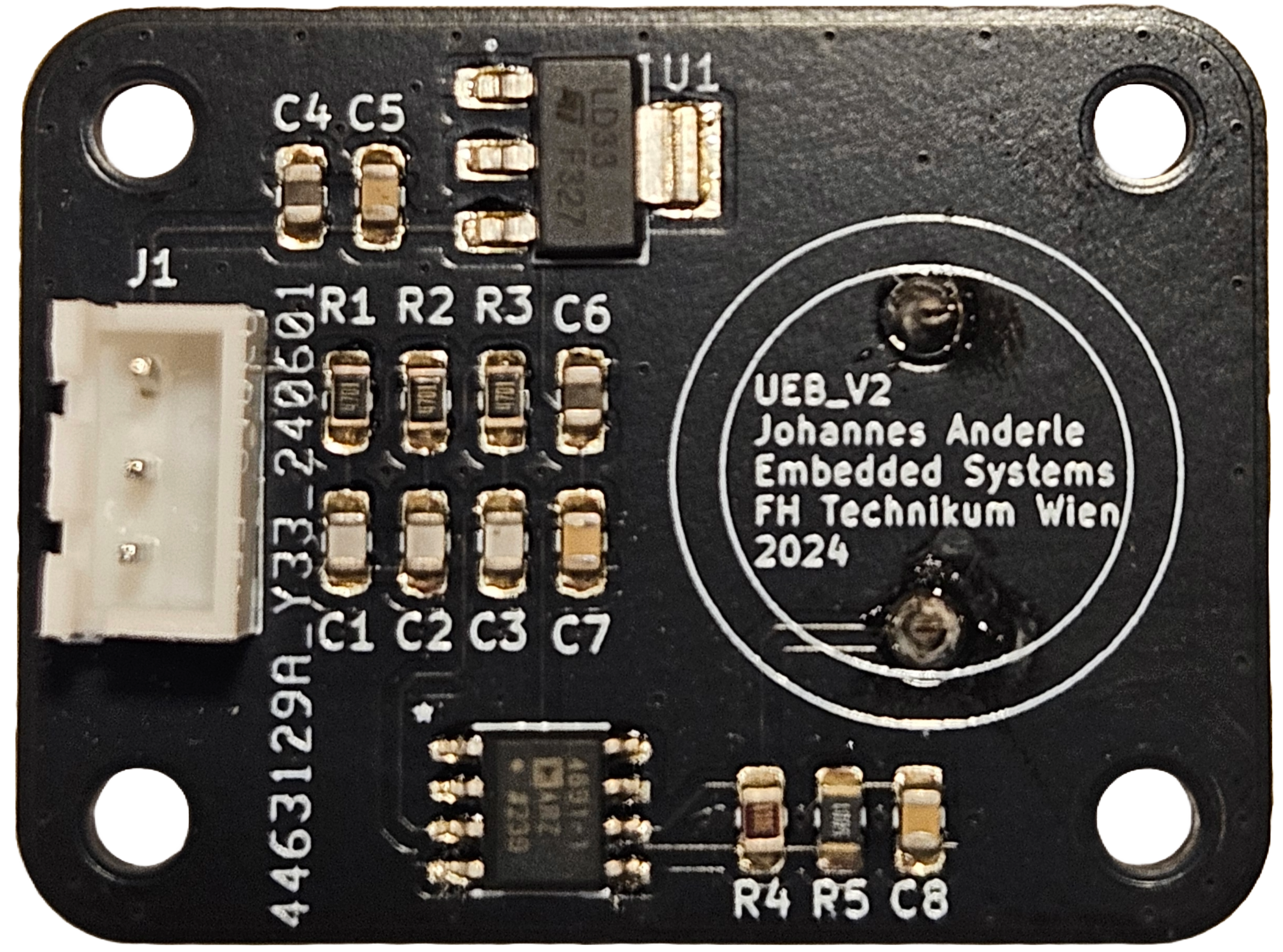
The resistors R4 and R5 have a reduced tolerance of 1% to improve comparability across different UEB_V2 boards. The ultrasound transducer is positioned at the white double circle located on the backside of the UEB_V2, as shown in the figure below.
First Transmitter PCB implementation - UEB V1 (based on a previous design by Mr. Gietler - reworked in 2024)
Heartbeat detection is based on the analysis of a reflected reference signal. To generate this signal, an ultrasonic transducer is required which converts an electrical signal into an acoustic signal.
Schematics
Similar to the AFE_V1, the UEB_V1 is supplied by 5V. However, the entire circuit operates on 3.3V, which is supplied by the LDO U2, as depicted in the figure below. This setup lowers the risk of damaging the LiteKitV2 in case of incorrect wiring.
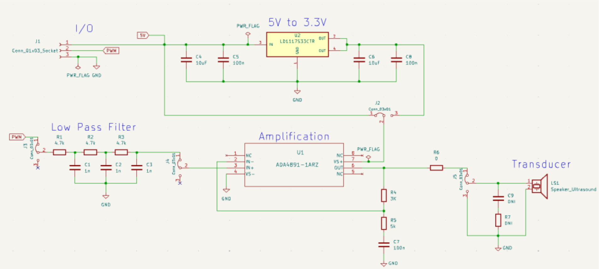
The LiteKitV2 output signal is a PWM , which is then transformed into an approximate sine wave signal by three low-pass filters connected in series (R1/C1, R2/C2, and R3/C3). The OPV U1, along with the external circuit R4/R5, is used to supply the necessary energy for the ultrasonic transducer. In this first version of the UEB_V1, there are multiple jumpers on the PCB that enable the circuit to be reconfigured. J2 allows the OPV to be powered with 5V to test the signal behaviour at higher voltage. By disconnecting pins 1 and 2 of J3, PWM signals from an external source can be input into the circuit via J3 pin 2. If the connection in J3 and J4 is removed and pin 1 of J3 is connected to pin 2 of J4, the low pass filter can be bypassed. External transducers can be connected via pins 1 and 3 of J5.
Layout
The layout places emphasis on the accessibility of the jumper and a logical signal flow from left to right, as illustrated in the figure below.
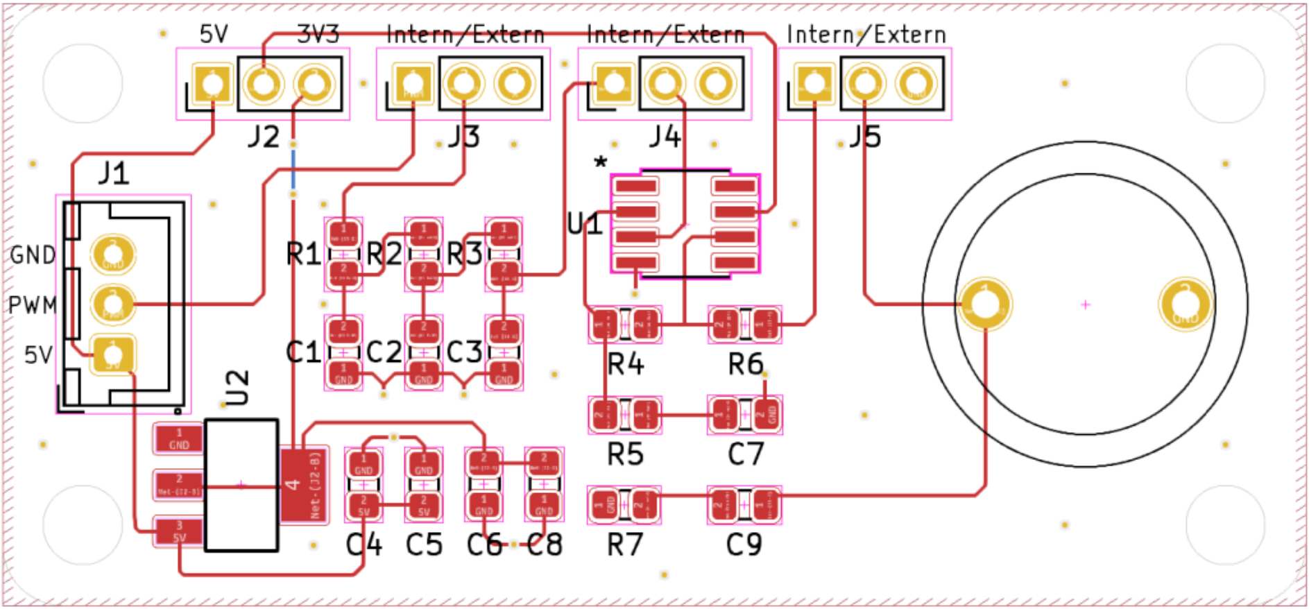
The low-pass filter components are selected to ensure that the cutoff frequency slightly exceeds the PWM frequency.
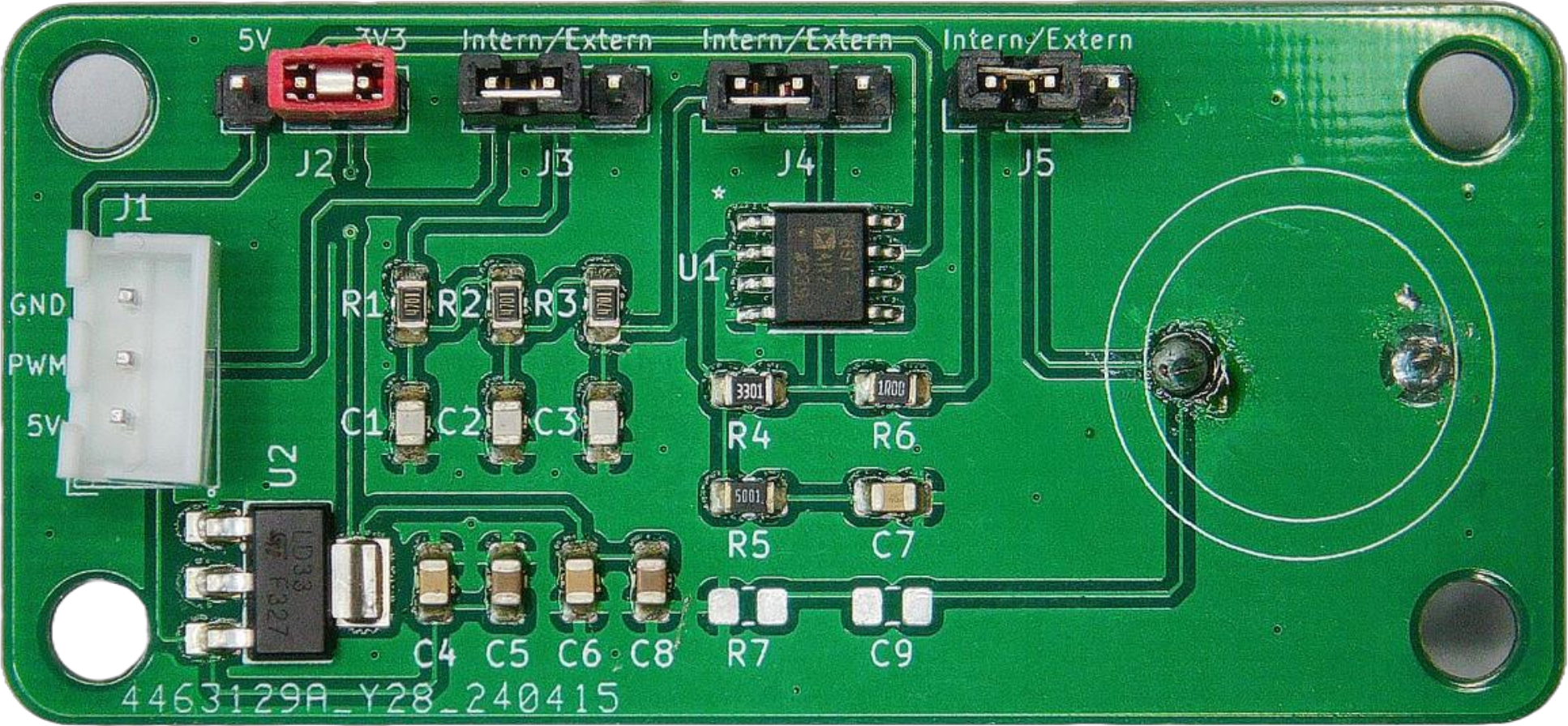
The ultrasound transducer is positioned at the white double circle located on the backside of the UFE_V1.
Fourth Analog Front-End further improvements - AFE V1 (by Mr. Anderle 2024)
As the previous AFE implementation described, the signal chain is functional for a single channel. To increase the measurement accuracy, the number of channels was increased to 3. The PCB AFE_V1 is a downsized and optimized version of the old PCB V4 to improve the setup further. The downsizing was mainly achieved by removing all non-essential circuit components. By switching to the OPV LTC1992, an external voltage reference is no longer required to adequately shift the output signal, as the LTC1992 has this function incorporated. The overvoltage protection circuit is no longer necessary because the operating voltage is set to 3.3V. Since the proper functionality of the circuit was verified, all test points, jumpers and potentiometers were removed. Lastly, the component layout was changed so that the assembly and installation of the PCB were as straightforward as possible.
Schematics
The schematic of the AFE_V1 is displayed in the following figure.
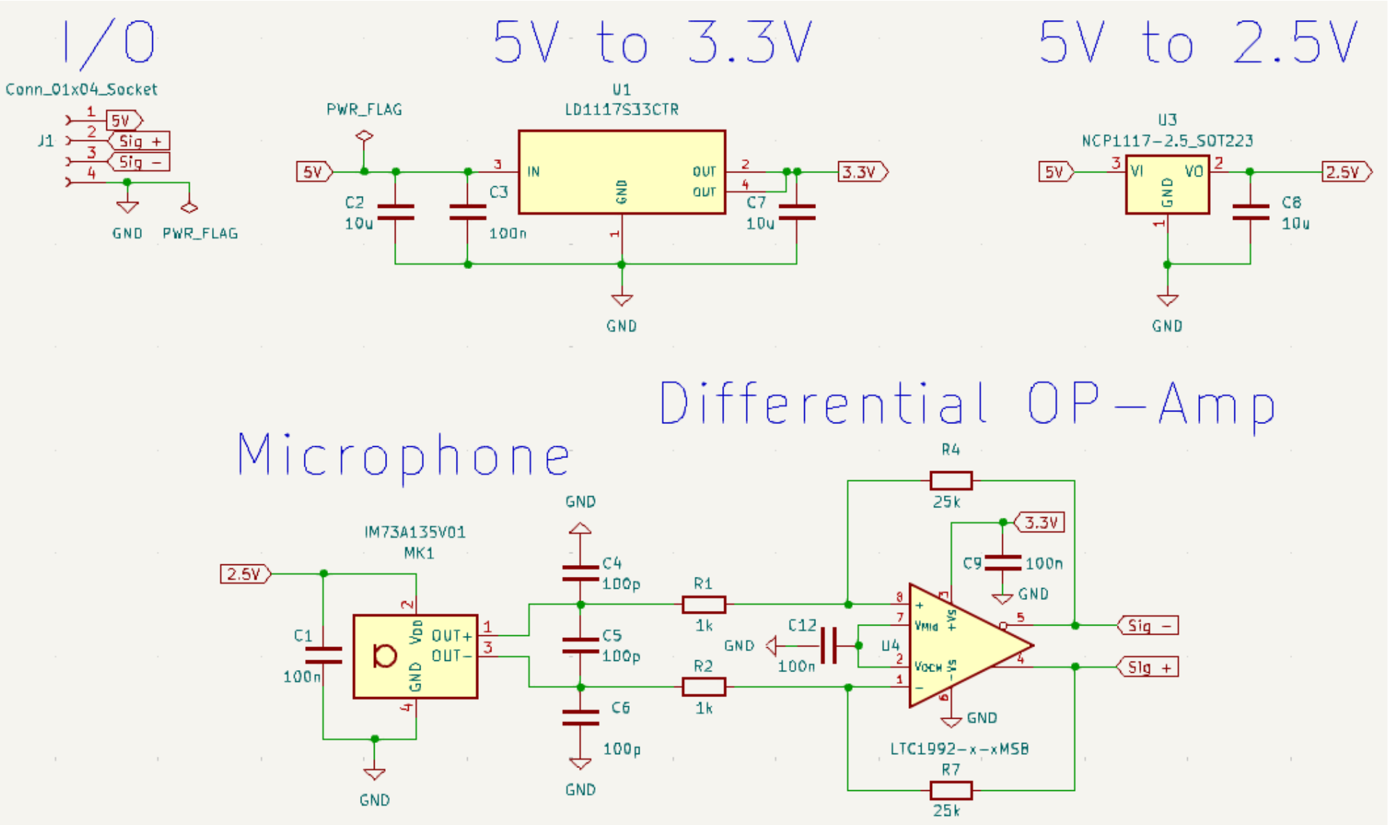
The key difference from the previous version of the AFE_V1 is the reduced number of components required, resulting in a significantly simplified circuit.
PCB Layout
The Layout of the components, shown in the figure below, reflects the simplification of the circuit.
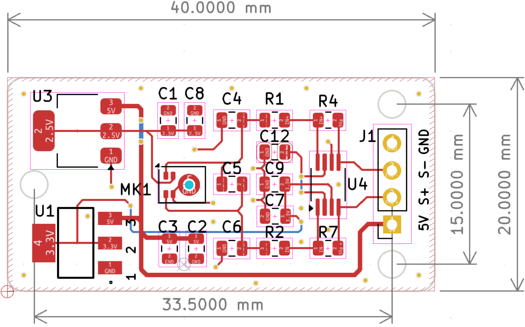
LDO U1 supplies the 3.3 V for the entire circuit, except for the microphone MK1, which is supplied by LDO U3. Capacitors C4, C5, and C6 are the microphone's capacitive loads; the other capacitors serve as voltage stabilization. Resistor pairs R1, R4, and R2, R7 provide the external circuitry for the OPV U4 to achieve the specified gain of 25.
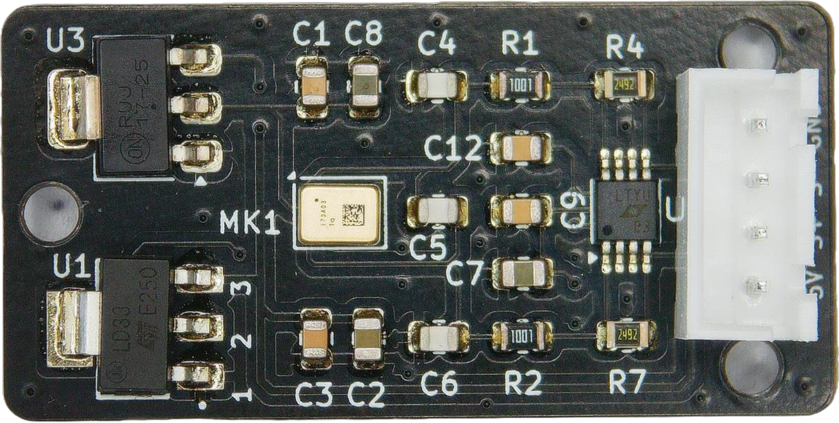
The figure above shows, the AFE_V1 is streamlined and more compact, making it easier to develop a sensor head.
Fourth Analog Front-End Implementation - AFE (by Mr. Anderle 2024)
The earlier version of the circuit board, Mic_PCM_V3, utilized two identical operational amplifiers (Op-Amps), one for each signal. Moreover, thick film resistors with a tolerance of 5 % were used. This configuration led to differences in the common mode voltage between the two signals. To address this issue, the Mic_PCM_V3 was updated to version 4.
Analog Front-End - Version 4: Schematic
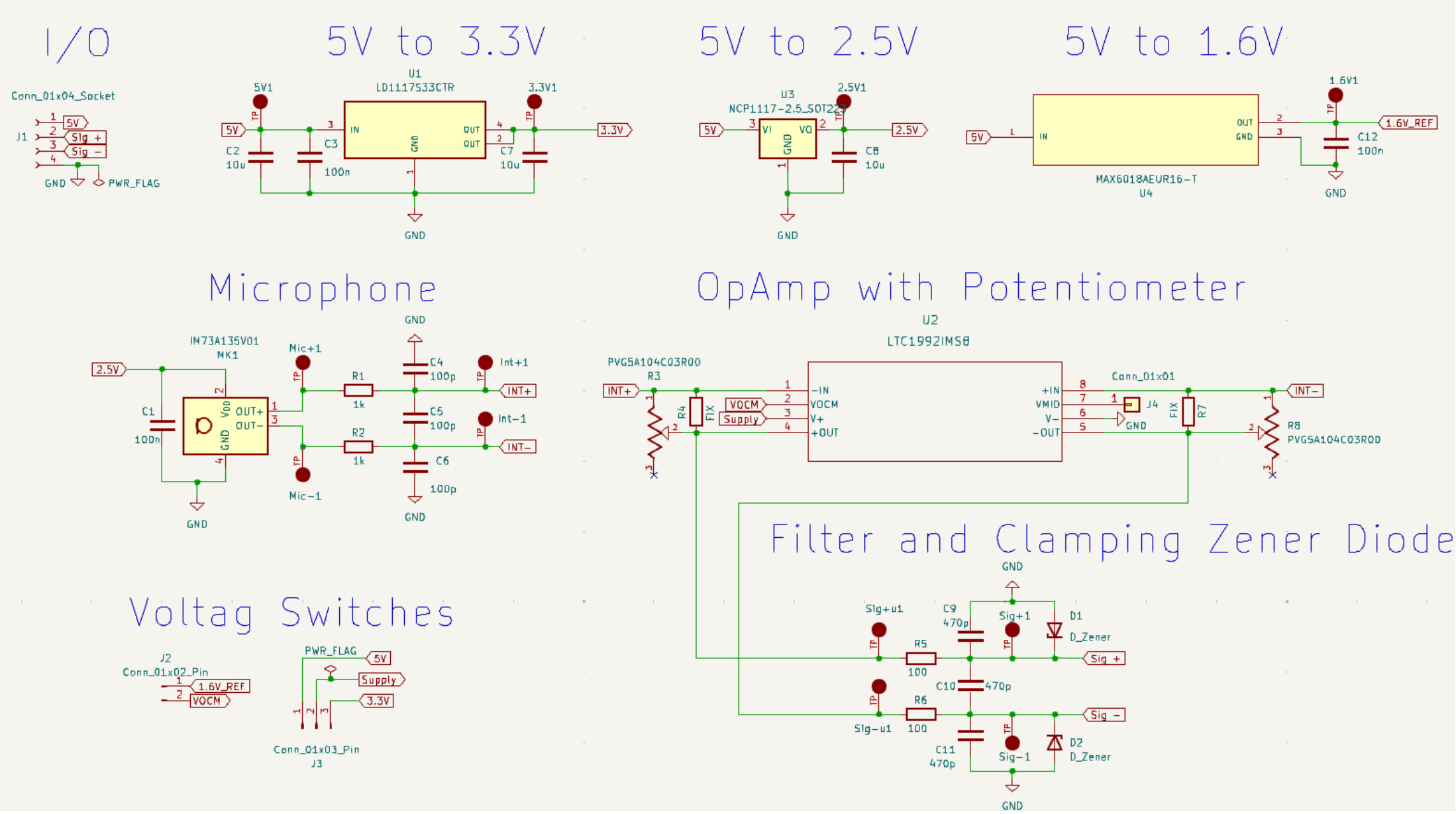
The major change in the new version of the AFE compared to its predecessor is the use of a differential Op-Amp, the LTC1992IMS8, labelled U2 in the schematic as shown in the figure below. This amplifier features a VMID pin that generates a voltage level equal to half the supply voltage. By feeding this voltage into the VOCM pin of the Op-Amp, the common mode output voltage of the Op-Amp is kept at half the supply voltage. As a result, the MAX6018 is no longer required for the final AFE design, although it is still included for evaluation and test purposes. The LTC1992IMS8 is compatible with both 3.3V and 5V operating voltages. The jumper marked as J3 offers the capability to modify the supply voltage. To establish a connection to the VOCM pin of the Op-Amp, jumper J2 is utilized for introducing 1.6V, or alternatively, a jumper wire can be connected between the VOCM pin and the VMID pin labelled J4. As the operational amplifier is able to operate with higher voltages, a protective circuit with two clamping diodes has been integrated. To evaluate the gain, a potentiometer or a fixed resistor can be used. Due to signal integrity issues, the ability to switch between these two options via pin headers has been removed. The selection is instead made by mounting the preferred component and omitting the other. An optional low-pass filter stage has also been added.
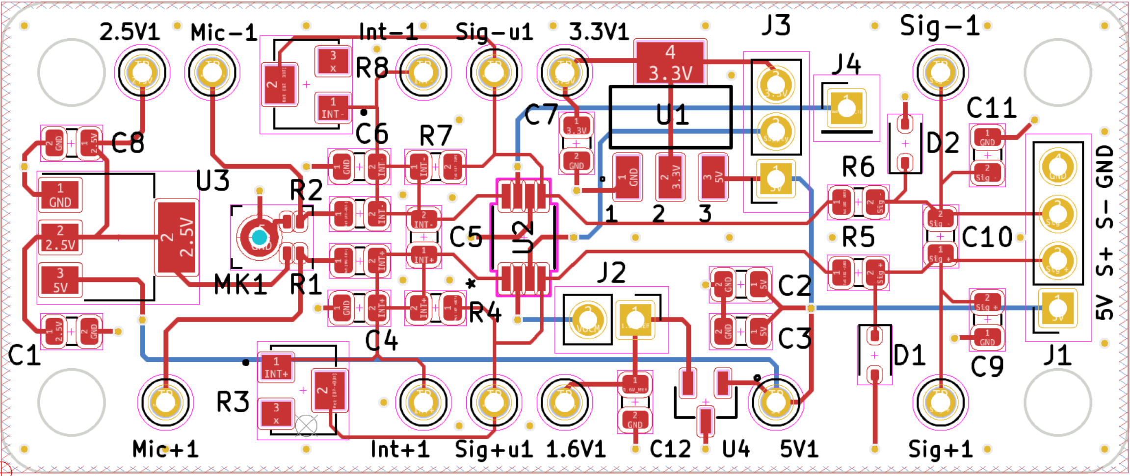
Analog Front-End - Version 4: PCB Layout
In the fourth version of the PCB, the formfactor was changed to a longer but slimmer design, to simplify mounting. The figure below shows that the test points have been relocated to the perimeter of the circuit board to improve access. Additionally, the components have been repositioned to guarantee identical lengths for both signal pathways.
The figure below displays the current configuration of the AFE. The locations designated for potentiometers, R3 and R8, are left vacant. Instead, 24.9kΩ resistors are placed at R4 and R7, which, combined with the 1kΩ resistors at R1 and R2, yield a gain of 24.9. The jumper at R3 is soldered with only two pins, allowing only a 3.3V voltage level to be supplied to the Op-Amp. As a result, the clamping diodes D1 and D2 become redundant. Additionally, the circuitry for 1.6V generation and the filter stage are not used. The resistors at R5 and R6 are bypassed with 0Ω resistors since there is no need for current limitation. All resistors employed in this setup have a precision of 0.1% tolerance.
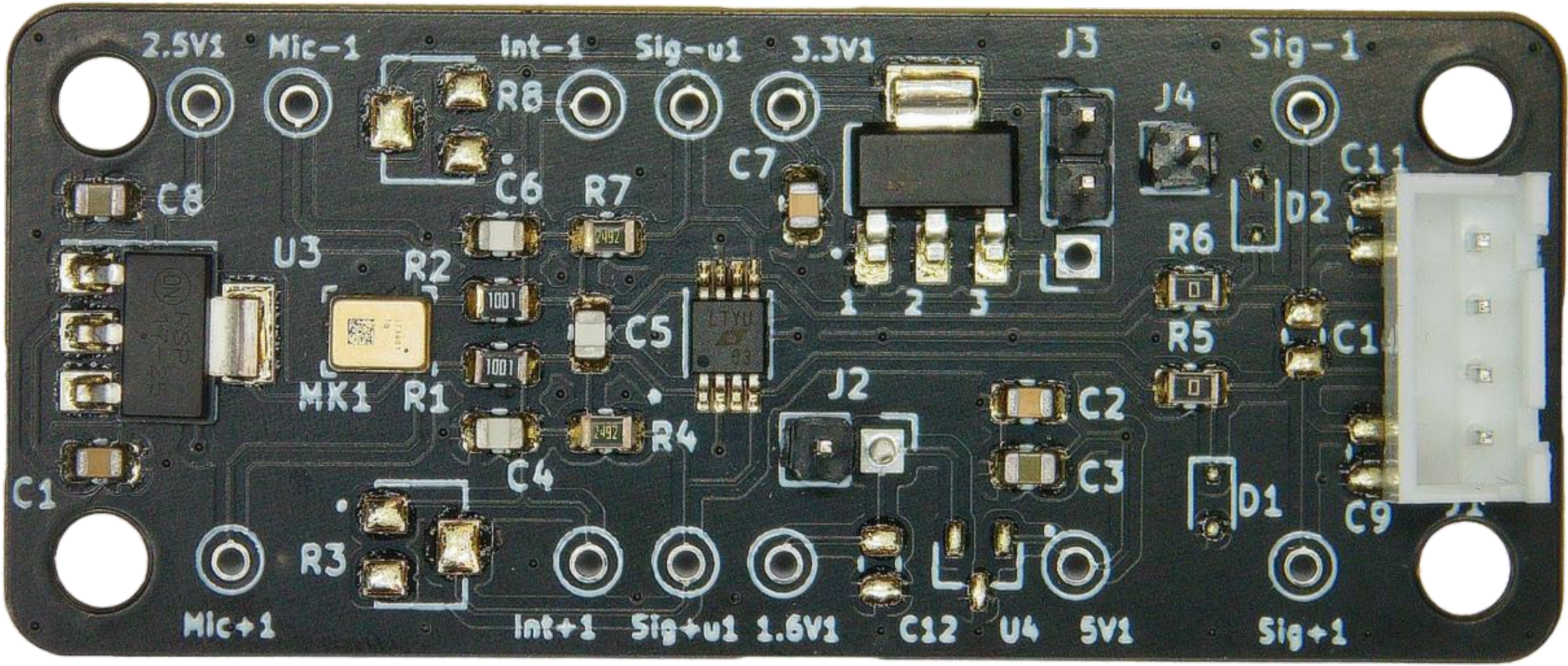
Note: The Jumper on J3 and the jumper wire between the left pin of J2 and J4 are not shown in this picture but are present on the prototype.
Second + Third Analog Front-End Implementation (based on Mr.Gneist - reworked by Mr.Anderle 2023)
The initial reworked PCB (V2) was created primarily for the evaluation of the OP-AMPs. Therefore, the PCB design was updated with several changes (V3 depicted in this chapter) to fully utilize the microphone and simplify the measurement process.
Schematic
The first improvement was to generate all the necessary voltages directly on the circuit board. This method ensures that all components are supplied with a stable and clean power voltage. The second major change affects the gain setting. Initially, the gain depended on the specific resistor installed, and changing the gain meant replacing and re-soldering the resistor. In the updated design, it is possible toggle between a fixed resistor and a potentiometer by adjusting the jumpers marked J2 to J6, as depicted in the following figure.
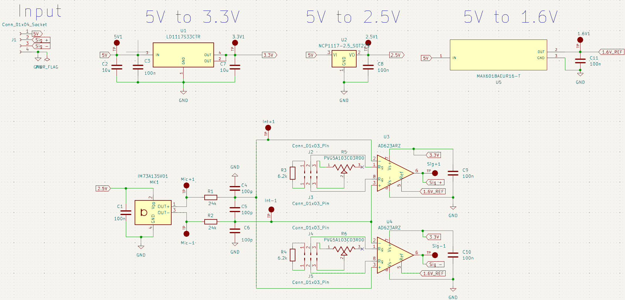
This change introduces the ability to adjust the gain in real time, enabling experimental fine-tuning to find the ideal gain for the intended application.
PCB Layout
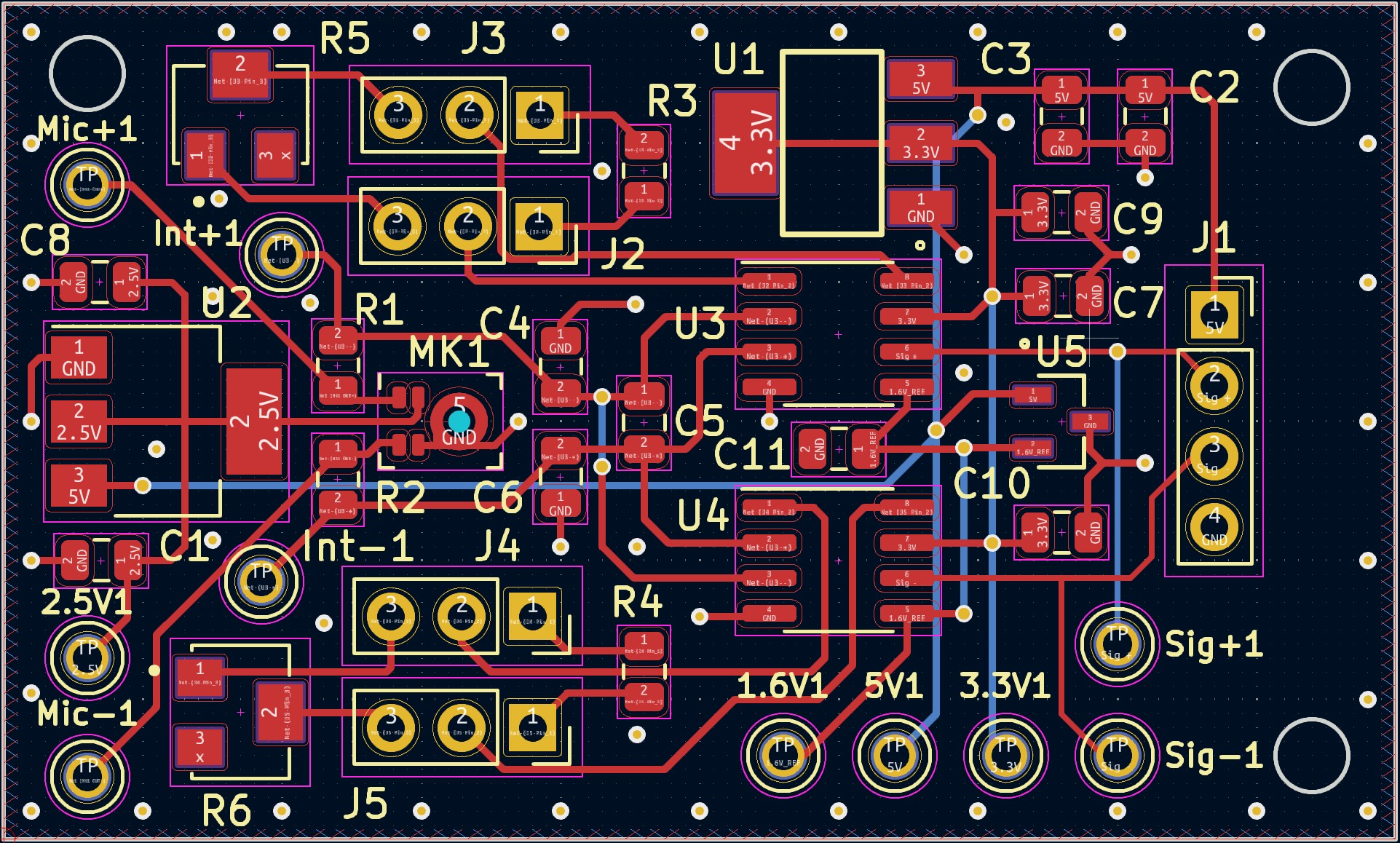
During the design of the circuit board, care was taken to ensure that the tracks carrying the differential signal were of equal length to guarantee signal integrity. The layout strategically places the microphone and OP-AMPs centrally, with test points located around the periphery for easy signal measurement. The arrangement of the pin headers for the jumpers is intuitive, clearly indicating which positions correspond to the potentiometer and which to the fixed resistor, as shown in the following figure.
The thickness of the PCB has been reduced to 1mm, which further improves the microphone's performance. Additionally, the design prioritizes compactness while including mounting holes for convenient installation, as shown in the following figure.
Operational Amplifier Analysis for further hardware revisions (by Mr.Anderle 2023)
With the change from the prototype microphones used by Mr. Gneist in his Master thesis to the IM73A135V01 microphone and the use of differential mode, a PCB redesign was necessary. The key part of the new design is the Operational Amplifier (OP-AMP), which amplifies the signal and directly adjusts it to the desired voltage of 1.6VDC. To guarantee the functionality and desired performance of the OP-AMP, the component underwent a thorough testing process. The initial version of the PCB was designed with multiple test points and the capability to input external signals for these evaluations. With a signal generator, we feed precisely defined signals into the OP-AMPs and assess their outputs. This approach enabled us to examine the behavior of the OP-AMPs in isolation, ensuring that the results were not affected by any interference from the microphone.
Baseline OP-AMP Test
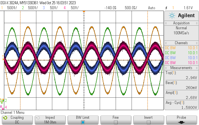
Initially, a baseline test was conducted using the following test parameters: Frequency set at 1kHz, Differential input voltage at 100mVPP (marked blue and red), Input offset voltage at 1.35VDC, and a Gain of 13.2. As shown in the following figure, the result displays the differential signals (marked in green and yellow), which exhibit the expected and desired behavior.
Higher Frequency Test
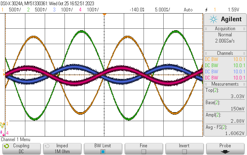
Given that this research project involves working with ultrasound in the 40kHz range, the test was replicated at an elevated frequency. The parameters for this test were set as follows: Frequency at 42kHz, differential input voltage at 100mVPP (represented in blue and red), input offset voltage at 1.35VDC, and a gain of 13.2. The findings, presented in the following figure, demonstrate that the differential output (depicted in green and yellow) exhibits a behavior akin to that observed in the basic test. However, a more pronounced phase shift and reduced output signal amplitude were noted. These observations suggest that the OP-AMP is operating near its maximum capacity.
Further evalution results of the used OP-AMP can be found within the "Results" section of this website.
First Analog Front-End Implementation (by Mr. Gneist 2022/23)
The initial prototype was designed by Mr. Gneist during his master thesis in 2022/23. His version conisted of three different stages. The first stage "Amplification Stage" creates an amplified single-ended signal out of the differential signal output of the Infineon MEMS microphone. The DC components of the differential signal output of the Infineon MEMS microphone is removed by using capacitors as a filter. The gain factor is set by standard resistors within the amplifier feedback. The factor depends on the amplitude of the reflected waves (after emitted by the transmitter part) and the characteristics of the used ADC. (voltage range) The second stage called "Offset Stage" utilizes an additional amplifier to shift the signal into the positive domain. This was done to ensure that the signal is in range of the Aurix EVADC input channels. The last stage is the "ADC protection Stage" and consists of standard silicon switching signal diodes acting as a cutoff for negative and too high voltages.
The schematics of this very first prototype is shown in the following figure.

This first front-end prototype was than integrated to a test configuration consisting of three hardware parts.
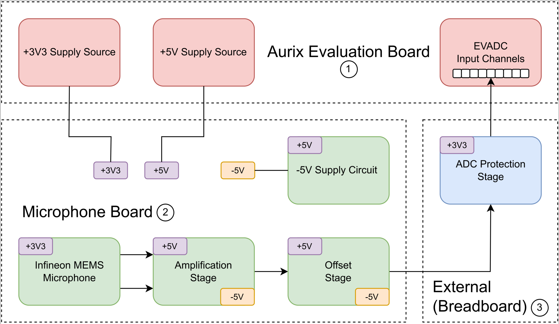
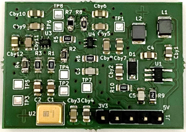
The block diagram previously shown illustrates parts two and three, which are essential for multichannel conversions, especially in solutions involving several microphones. The Aurix Evaluation Board plays a pivotal role, providing both +3V3 and +5V power to the Microphone Board and the external ADC Protection Stage. It also samples the modified and protected output signal from the Infineon MEMS microphone. Additionally, it facilitates the transmission of measurements to a PC via an interface, although this is not depicted in the block diagram since the focus is on parts two and three. The Microphone Board, another crucial component, alters the output of the Infineon MEMS microphone so it can be processed by an EVADC input channel. It also includes a -5V Supply Circuit, necessary for the Amplification Stage and Offset Stage, which require a negative supply. Lastly, the external component, which is typically a breadboard, serves both a mechanical and functional purpose. It provides a platform for mounting the Microphone Board and integrates an ADC Protection Stage. This stage is vital as it safeguards the EVADC input channel from potential damage due to voltages that fall outside the specified range. The upcoming pictures show the assembled PCB with its components soldered as well as a foto of the first measurement setup consisting of three MEMS microphones attached to an Aurix LiteKit development board.
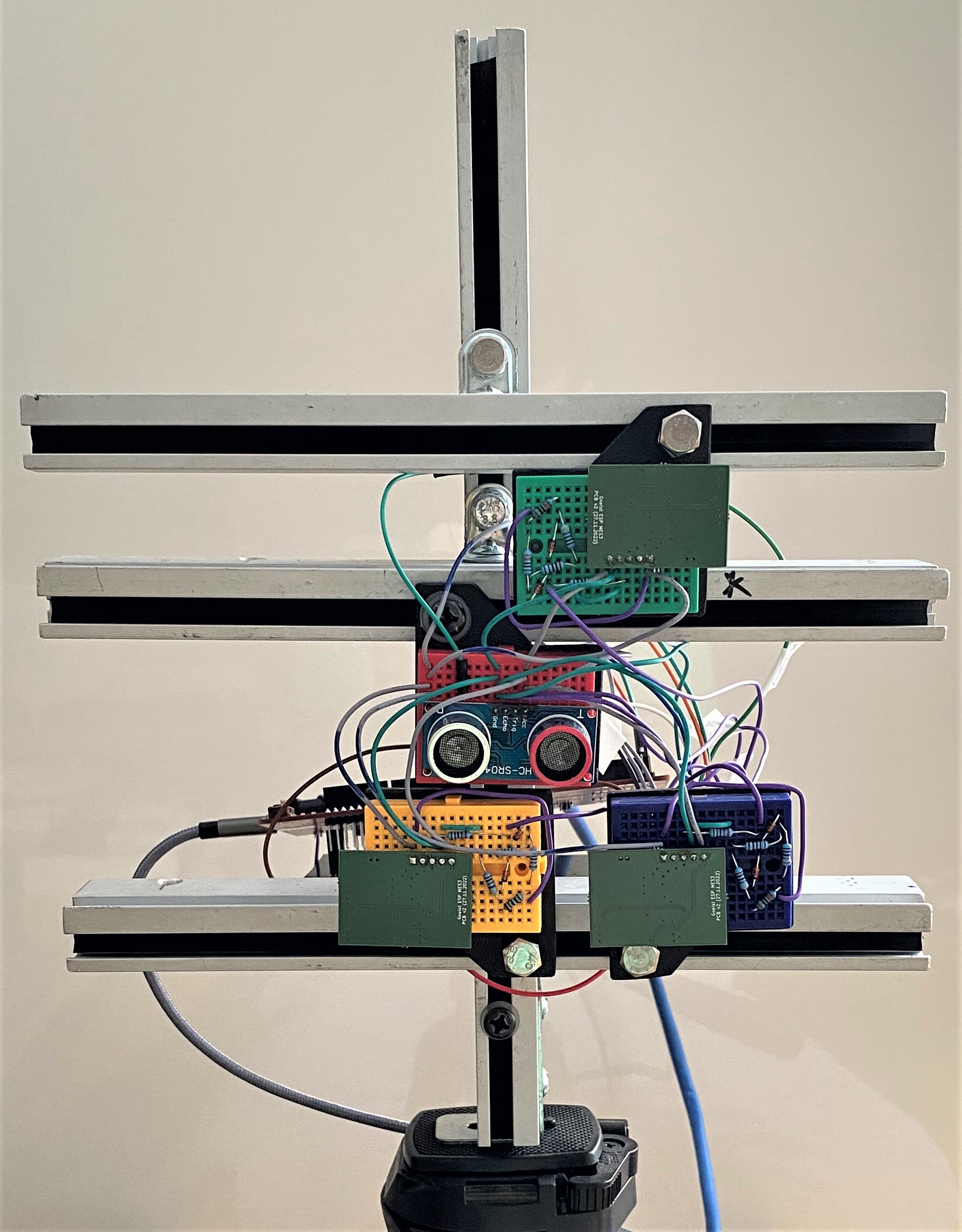
In the foto below the whole target system is presented from the front. The respective arrangement of the modules, forming a triangle, can be seen. As ultrasound transmitter, the sender part of an ultrasonic ranging module is used, whose capsule edge is highlighted in red. This is the defined centre of the target system.
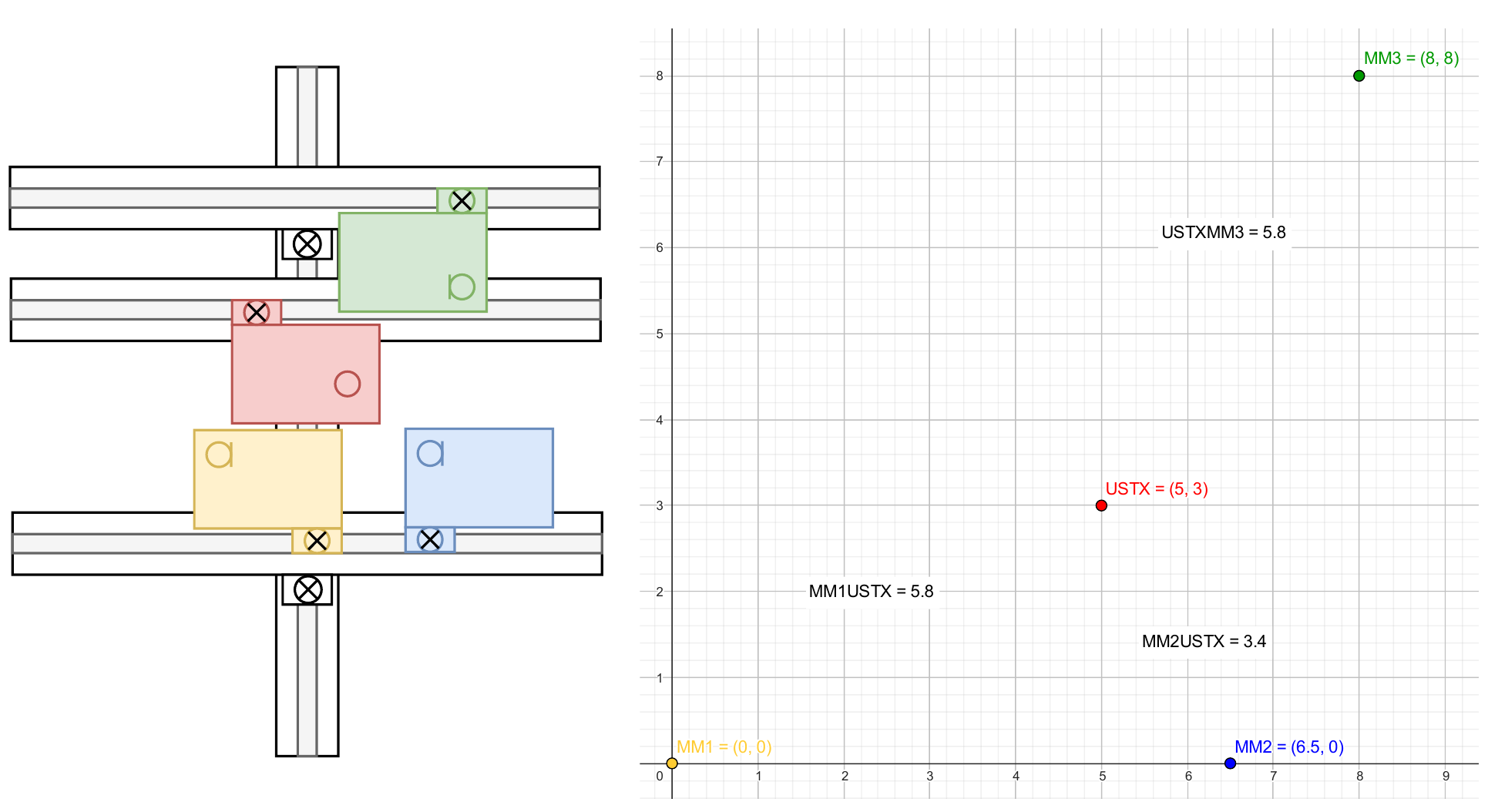
Arrangement of the Modules
The ultrasound transmitter module (USTX) has been defined as centre of the arrangement. Around this centre, the Microphone Modules (MM) have been positioned as illustrated schematically in the upcoming figure on the left side. The irregular arrangement has been selected to reduce the probability of null-point issues. The ABS plastic plate to mount the LiteKit (D within the figure) is not shown in this draft. On the right side of the respective figure, the centre of each Module (centre of acoustical ports of the microphones / centre of the ultrasound transmitter capsule) and their relation are drawn in a Cartesian coordinate system (in cm). The yellow Microphone Module has been selected as reference in the diagram and set to position (0/0).